Systems and Methods to Provide Enhanced Diode Bypass Paths

a diode bypass and bypass path technology, applied in the field of systems and methods to provide enhanced diode bypass paths, can solve problems such as current and voltage spikes through the bypass diod

Active Publication Date: 2012-08-09
NEWLIGHT CAPITAL LLC
View PDF21 Cites 172 Cited by
  • Summary
  • Abstract
  • Description
  • Claims
  • Application Information

AI Technical Summary

Benefits of technology

[0007]In one embodiment, systems and methods are herein disclosed for efficiently allowing current, or a bypass current, to bypass a group of solar cells having one or more malfunctioning or shaded solar cells without overwhelming a bypass diode. This can be done using a switch (e.g., a metal-oxide semiconductor field-effect transistor) connected in parallel with the bypass diode. By turning the switch on, a majority of the bypass current can be routed through the switch, which is configured to handle larger currents than the bypass diode is designed for, and a minority of the current can be routed through the bypass diode.
[0015]In one embodiment, a method for controlling electric currents in a photovoltaic system includes: charging a first capacitor, in response to bypass current passing through a parasitic diode of a transistor connected in parallel to an output of a group of solar cells, using a first diode powered by a voltage drop across the parasitic diode; converting a first voltage across the first capacitor to generate a second voltage; charging a second capacitor using the second voltage; powering a controller using the second capacitor; and activating the transistor using the controller to reduce a voltage drop across the transistor, after the first capacitor and the second capacitor are charged to a predetermined level. In one embodiment, the first diode is not conductive when the transistor is activated, and the method also includes discharging the first capacitor and the second capacitor after the voltage drop across the transistor is reduced, and deactivating the transistor after the first capacitor and the second capacitor are discharged to a predetermined level.

Problems solved by technology

This causes a current and voltage spike through the bypass diode.

Method used


Image

  • Systems and Methods to Provide Enhanced Diode Bypass Paths
  • Systems and Methods to Provide Enhanced Diode Bypass Paths
  • Systems and Methods to Provide Enhanced Diode Bypass Paths

Examples


Embodiment Construction

[0026]The following description and drawings are illustrative and are not to be construed as limiting. Numerous specific details are described to provide a thorough understanding. However, in certain instances, well known or conventional details are not described in order to avoid obscuring the description. References to one or an embodiment in the present disclosure are not necessarily references to the same embodiment; and, such references mean at least one. Similarly, various requirements are described which may be requirements for one embodiment but not other embodiments. Further, unless excluded by explicit description and / or apparent incompatibility, any combination of various features described in this description is also included here.

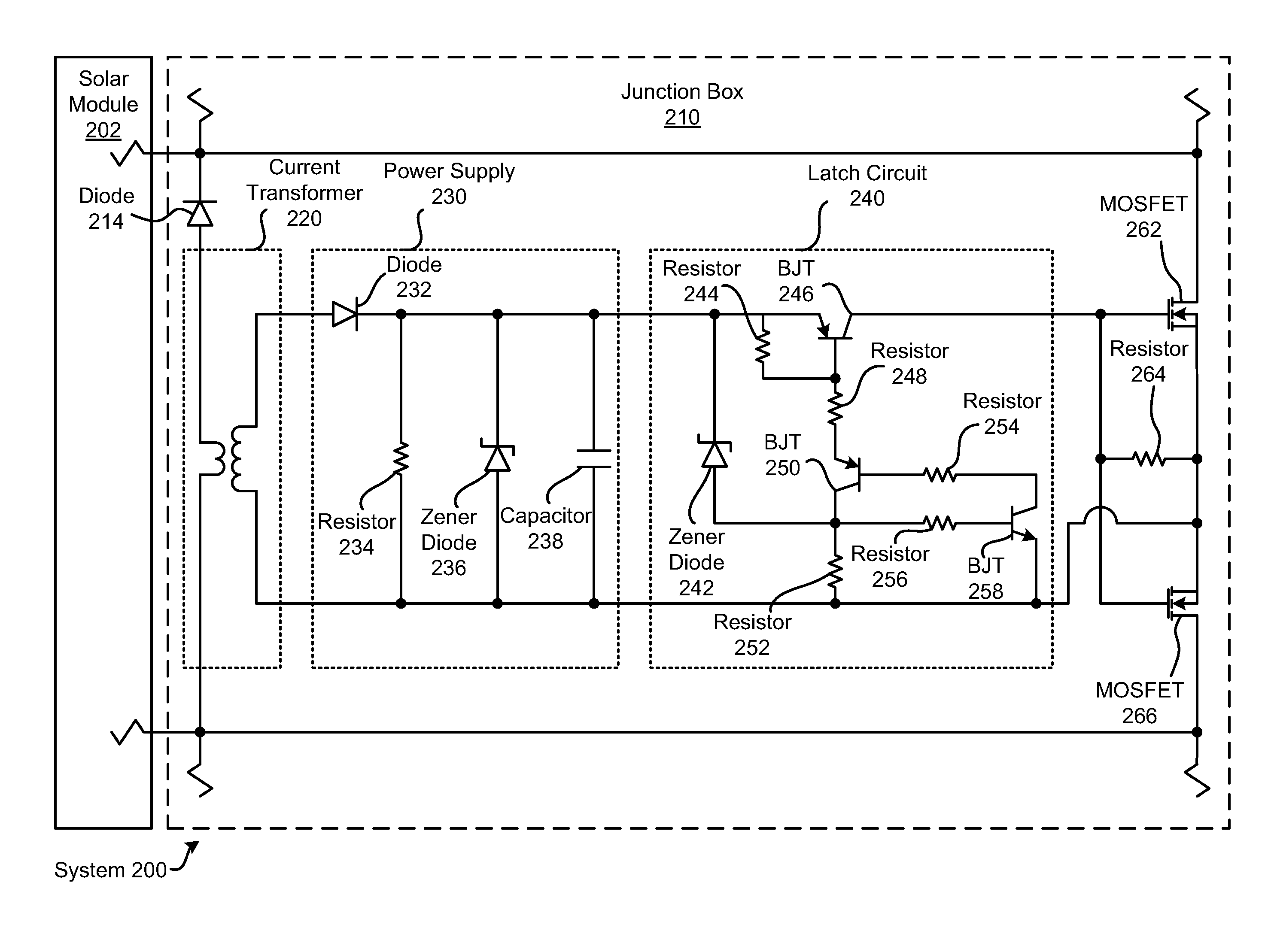
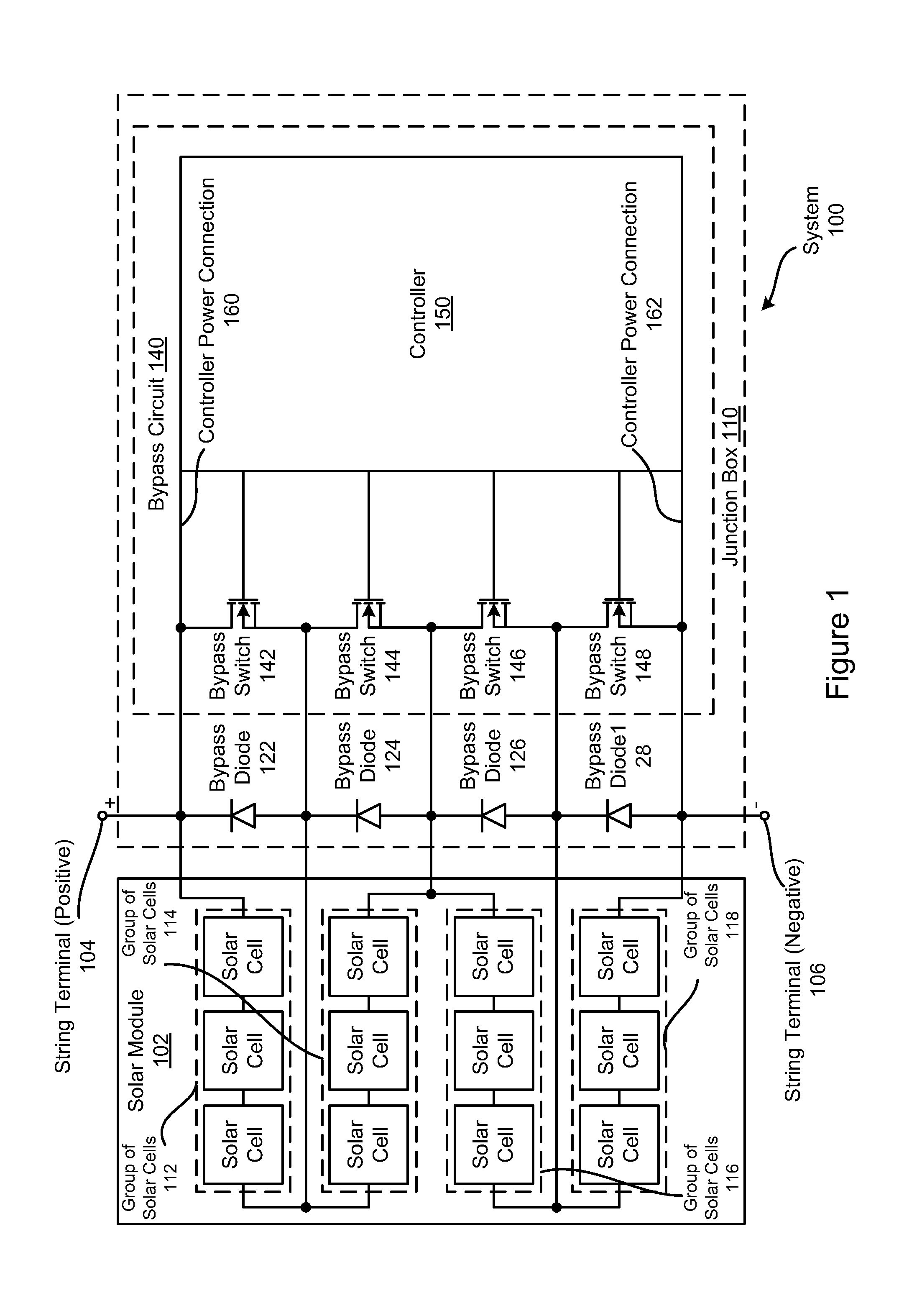
[0027]FIG. 1 illustrates an embodiment of switches connected in parallel to bypass diodes. The system 100 illustrated in FIG. 1 includes a solar module 102 having four groups of solar cells 112, 114, 116, 118. Each group of solar cells 112, 114...


PUM


Abstract

Systems and methods are herein disclosed for efficiently allowing current to bypass a group of solar cells having one or more malfunctioning or shaded solar cells without overwhelming a bypass diode. This can be done using a switch (e.g., a MOSFET) connected in parallel with the bypass diode. By turning the switch on and off, a majority of the bypass current can be routed through the switch, which is configured to handle larger currents than the bypass diode is designed for, leaving only a minority of the current to pass through the bypass diode.

Description

CROSS-REFERENCE TO RELATED APPLICATIONS[0001]The present application claims the benefit of the Prov. U.S. Pat. App. Ser. No. 61 / 440,342, filed Feb. 7, 2011 and entitled “Systems and Methods to Provide Enhanced Diode Bypass Paths,” the disclosure of which is incorporate herein by reference.[0002]The present application relates to U.S. patent application Ser. No. 12 / 724,371, filed Mar. 15, 2010 and entitled “Systems and Methods to Provide Enhanced Diode Bypass Paths,” the disclosure of which is incorporate herein by reference.FIELD OF THE TECHNOLOGY[0003]At least some embodiments of the disclosure relate to limiting current in bypass diodes of a solar energy generating system.BACKGROUND[0004]Solar cells can be connected in series to form strings. When one or more solar cells in the string malfunction or are shaded from sunlight, the malfunctioning or shaded solar cells become highly resistive. As a result, other solar cells in the string may not generate enough voltage to overcome the...

Claims


Application Information

Patent Timeline
Patent Type & Authority Applications(United States)
IPC IPC(8): H01L31/042H03K17/56
CPCH03K17/082Y02E10/50H01L31/02021H02J7/35H02J2207/10H02J1/10H02J9/062H02M3/04H02J7/345
Inventor AVRUTSKY, MORDECHAY
Owner NEWLIGHT CAPITAL LLC
Why Eureka
Try Eureka