Control circuit and method for controlling a power semiconductor switch

a control circuit and power semiconductor technology, applied in the direction of electronic switching, oscillator generator, pulse technique, etc., can solve the problems of signal delay, high power loss of igbt, and the need for space, so as to reduce the influence and the problem of parasitic capacitors, and the effect of easy keeping the response time constan

Active Publication Date: 2012-08-09
POWER INTEGRATIONS INC
View PDF4 Cites 36 Cited by
  • Summary
  • Abstract
  • Description
  • Claims
  • Application Information

AI Technical Summary

Benefits of technology

[0025]Advantageously, the driving circuit and the method according to the present invention make it substantially easier to keep the response time constant in a wide range of values possible for the collector-emitter voltage. The influence and the problem of parasitic capacitors are able to be decreased. The driving circuit and the method of the present invention are suitable both for turning on a power semiconductor switch into the short circuit (so-called short circuit of type 1), and for the case of a short circuit in the ON state of the semiconductor switch (so-called short circuit of type 2).
[0026]According to an especially preferred embodiment, the driving circuit of the present invention has a plurality of ser

Problems solved by technology

This results in a very high power loss of the IGBT.
Because of these high values for resistors RVCE1, RVCE2, RVCE3, and the parasitic input capacitor CAP of the signal-processing unit or of comparator COMP, (including their wiring), a relatively high time constant or response time results for the circuit configuration, leading to a corresponding signal delay.
The disadvantages in so doing are an additionally necessary space requirement, a decrease in the maximally permitted operating temperature, an increased number of components, increased costs and, as a rule, reduced reliability.
A further disadvantage in using such a compensated voltage divider is that, given a monolithic integration of comparator COMP and control unit CONTROL of the signal-processing unit, a suppression time, in which the VCE monitoring is deactivated, must be set subsequent to the comparison of the measured collector-emitter voltage to the setpoint value carried out by comparator COMP, thus, must be carried out within or with the aid of control unit CONTROL.
However, this requires additional measures for setting the suppression time, such as a digital programming or further connecting pins at the monolithically integrated signal-processing unit.
This can lead to an unintentional restriction with respect to the optimal design and operation of power semiconductor switch S, even though the short-circuit energy can be held constant to a great extent in circuit configuration 1′ sho

Method used


Image

  • Control circuit and method for controlling a power semiconductor switch
  • Control circuit and method for controlling a power semiconductor switch
  • Control circuit and method for controlling a power semiconductor switch

Examples


Embodiment Construction

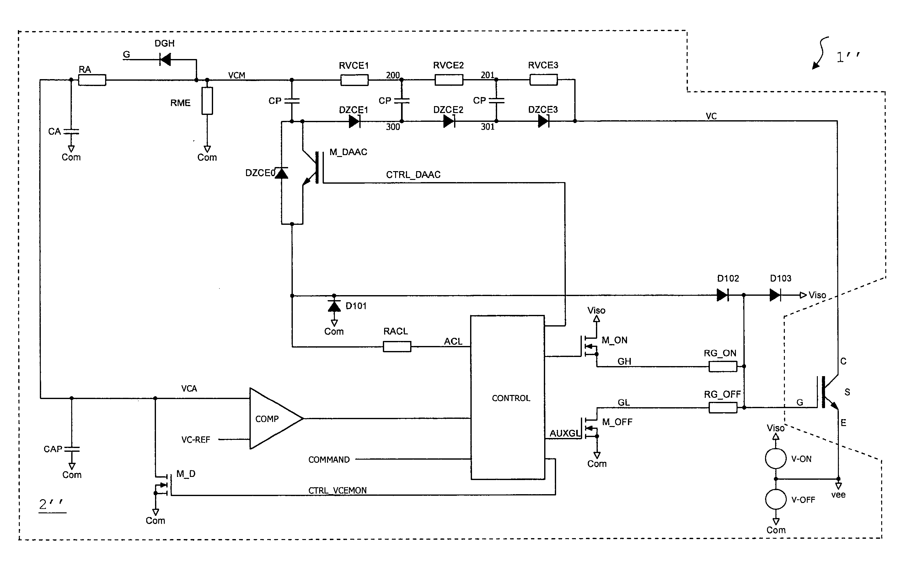
[0020]The object of the present invention is to provide a driving circuit which is improved compared to the driving circuits described at the outset and a method for driving a power semiconductor switch which is improved compared to the methods described at the outset, by which the influence of parasitic capacitors is able to be reduced, in particular, is able to be minimized. It is further an object of the invention to provide a driving circuit and a method for driving a power semiconductor switch of less complexity, particularly of reduced complexity compared to the driving circuit and the corresponding method described in connection with FIG. 3. A further object of the present invention is to provide a driving circuit and a method for driving a power semiconductor switch in which the thermal stress of the components is low, in particular, is reduced or minimized compared to the driving circuits and methods described at the outset. Furthermore, it is an object of the invention to ...


PUM


Abstract

A driving circuit for driving a power semiconductor switch wherein at least one semiconductor device being provided which is implemented in such a way that it is operated in breakdown in response to the exceeding of a specific collector-emitter voltage of the power semiconductor switch, an output of the at least one semiconductor device being connected via a conductive interconnect to a terminal between the resistors of the resistor series circuit or to the resistor-series-circuit output which is connected to the signal processing unit, and the breakdown voltage of the at least one semiconductor device being selected in such a way that the potential at the output of the at least one semiconductor device is greater than the potential at the gate of the power semiconductor switch in its ON state. The invention further relates to a method for driving a power semiconductor switch.

Description

REFERENCE TO RELATED PATENT APPLICATIONS[0001]This application claims the priority of the European Patent Application No. 11 002 165.6, which was filed on Mar. 16, 2011, and whose entire disclosure is herewith incorporated by reference.FIELD OF THE INVENTION[0002]The present invention relates to a driving circuit and a method for driving a power semiconductor switch according to the preamble of the independent claims.BACKGROUND INFORMATION[0003]When working with power semiconductor devices, especially power semiconductor devices having a MOSFET control head, as a rule, it takes a certain time until the power semiconductor device (hereinafter also component or element, for short) is completely turned on and the voltage, which drops across the load terminals or power terminals of the device, and in the case of IGBTs, corresponds to the collector-emitter voltage usually denoted by VCE, has fallen to the desired low values. In the event of a fault, e.g., if an IGBT is turned on when the...

Claims


Application Information

Patent Timeline
IPC IPC(8): H03K3/00
CPCH03K2217/0027H03K17/0828
Inventor THALHEIM, JANGARCIA, OLIVIER
Owner POWER INTEGRATIONS INC
Why Eureka
Try Eureka