Solid-state image pickup device

Inactive Publication Date: 2012-08-09
PANASONIC CORP
View PDF4 Cites 9 Cited by
  • Summary
  • Abstract
  • Description
  • Claims
  • Application Information

AI Technical Summary

Benefits of technology

[0014]With the above structure, only the switch is added, but there is no need to add dummy pixels. Accordingly, it is possible to obtain the data for correcting the vertical fixed pattern noise with accuracy, while restricting the increase of layout area.
[0015]The above-described solid-state imaging apparatus may further comprise: a reset unit resetting each capacitor by applying a predetermined voltage thereto. Also, the above-described solid-state imaging apparatus may further comprise: an input unit inputting a predetermined potential to each unit column circuit while the electrical connection is shut off by the switch. With the above structure, it is possible to stabilize the input potential to the unit column circuit, making it possible to obtain the correction data with more accuracy.
[0016]In the above-described solid-state imaging apparatus, the predetermined potential may be a ground potential. With this structure, it is possible to improve the accuracy of the data for correcting the vertical fixed pattern noise because a constant voltage source and a ground line have low impedance.
[0017]In the above-described solid-state imaging apparatus, the predetermined potential may be a potential of current received by a bonding pad that is not electrically connected to any line that is connected

Problems solved by technology

This causes a fixed column pattern noise appearing like a vertical line.
Thus the method of increasing the pixel size

Method used


Image

  • Solid-state image pickup device
  • Solid-state image pickup device
  • Solid-state image pickup device

Examples


first embodiment

[1] First Embodiment

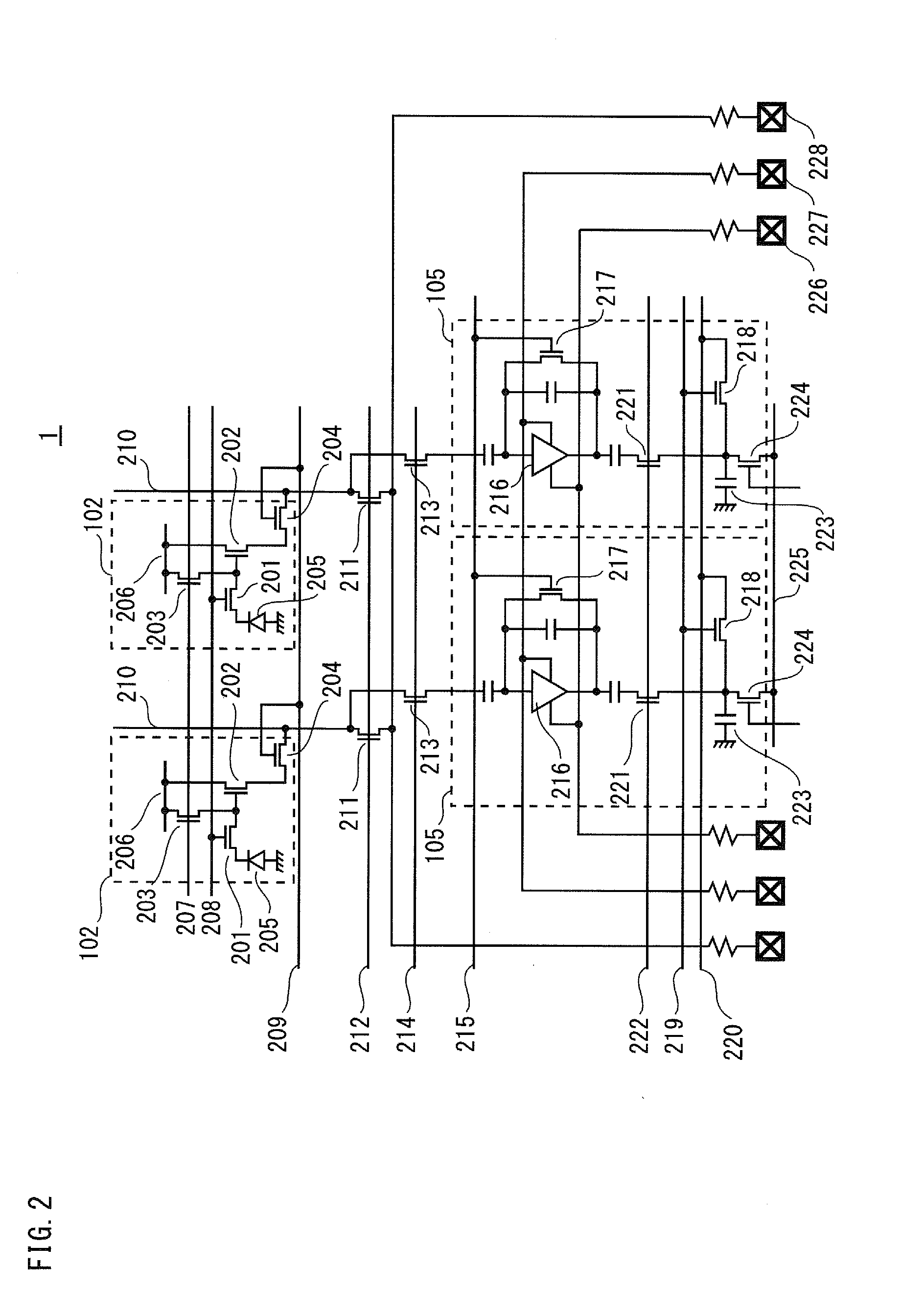
[0039]The following describes a solid-state imaging apparatus of the first embodiment of the present invention. The solid-state imaging apparatus of the present embodiment is characterized by a means for shutting off signals that are to be input from the vertical common signal lines to the unit column circuits. In this shut-off state, data for correcting the vertical fixed pattern noise is obtained.

(1-1) Structure of Solid-State Imaging Apparatus

[0040]First the structure of the solid-state imaging apparatus in the present embodiment is explained.

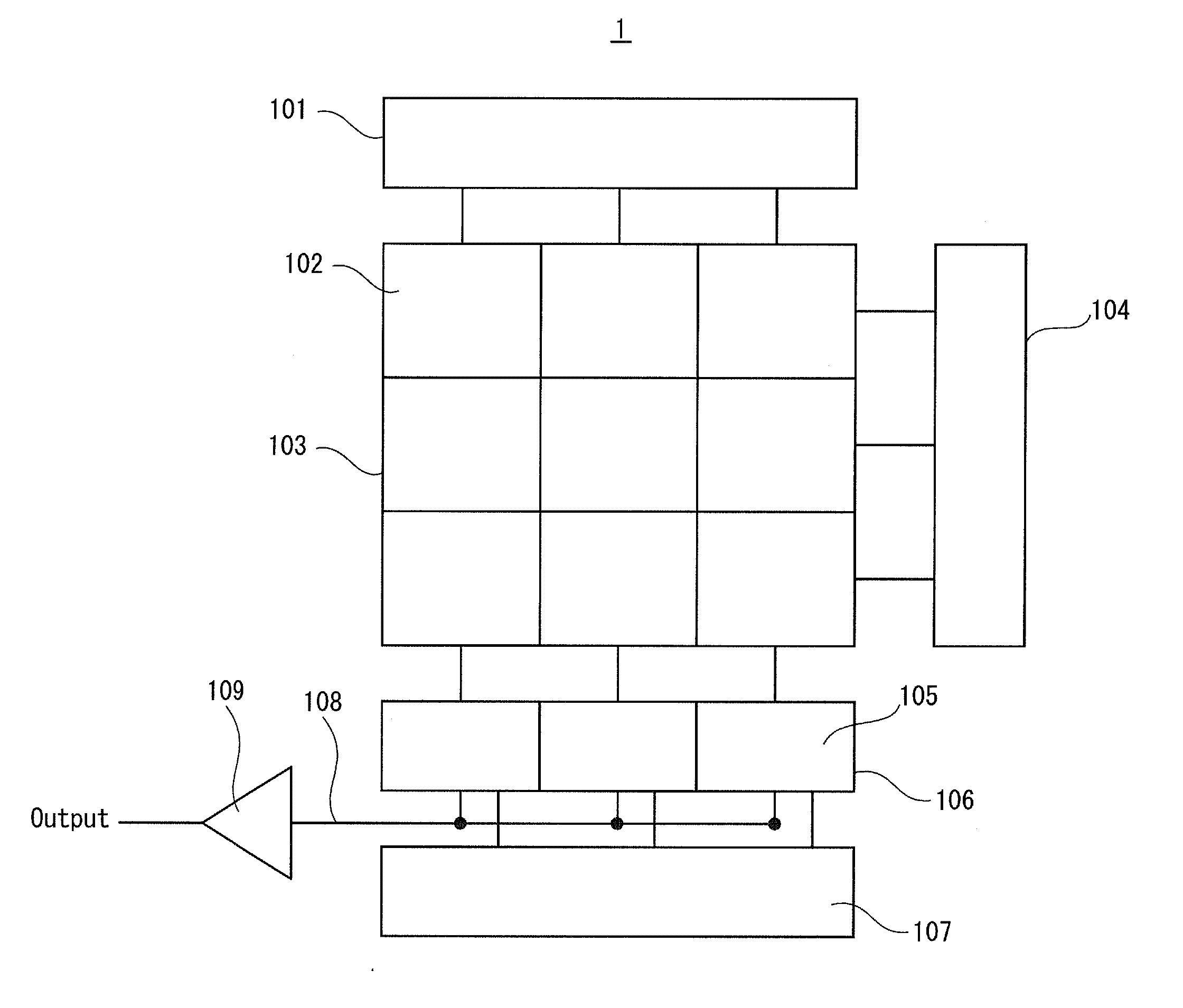
[0041]FIG. 1 illustrates the main structure of the solid-state imaging apparatus in the present embodiment. As shown in FIG. 1, a solid-state imaging apparatus 1 includes a current source circuit block 101, a pixel array 103, a vertical scanning circuit 104, a column circuit block 106, a horizontal scanning circuit 107, a horizontal common signal line 108, and an output amplifier 109.

[0042]A multiplicity of pixel cells 10...

second embodiment

[2] Second Embodiment

[0087]The following describes the second embodiment of the present invention. The solid-state imaging apparatus of the present embodiment has approximately the same structure as the solid-state imaging apparatus of the first embodiment, except that a plurality of photodiodes are provided in one pixel cell. In the following, the structure is explained centering on the difference.

[0088]FIG. 4 is a circuit diagram illustrating the structure of the solid-state imaging apparatus in the present embodiment. As shown in FIG. 4, a solid-state imaging apparatus 2 of the present embodiment has a so-called 2-pixel 1-cell structure in which two photodiodes 205 share the pixel source follower transistor 202, pixel reset transistor 203, and pixel selection transistor 204.

[0089]Even with the 2-pixel 1-cell structure, if the vertical common signal line switch transistor 213 is provided and operated in the same manner as in the first embodiment, it is possible to obtain, with acc...

third embodiment

[3] Third Embodiment

[0091]The following describes the third embodiment of the present invention. The solid-state imaging apparatus of the present embodiment has approximately the same structure as the solid-state imaging apparatus of the second embodiment, except that the data for correcting the vertical fixed pattern noise is obtained by applying a fixed voltage as input to the unit column circuits 105. In the following, the structure is explained centering on the difference.

[0092]FIG. 5 is a circuit diagram illustrating the structure of the solid-state imaging apparatus in the present embodiment. FIG. 6 is a timing chart illustrating the operation of the solid-state imaging apparatus in the present embodiment.

[0093]As shown in FIG. 5, a solid-state imaging apparatus 4 of the present embodiment further includes a column circuit input fixation bias line 502 and column circuit input fixation transistors 503 in addition to the structural elements of the first embodiment. The column ci...


PUM


Abstract

During the vertical blanking period, first the vertical common signal line switch transistor 213 is turned OFF, then the clamp transistor 218 is turned ON, thereby fixing the sample/hold capacitor 223 to the clamp potential. Also, the column amplifier reset transistor 217 is turned ON, and the column amplifier 216 is reset. Next, the column amplifier reset transistor 217 and the clamp transistor 218 are turned OFF, and the unit column circuit 105 is kept to the clamp state. In this state, the sample/hold transistor 221 is turned OFF, and the sample/hold capacitance 223 is read. The read data is used as the data for correcting the vertical fixed pattern noise.

Description

TECHNICAL FIELD[0001]The present invention relates to a solid-state imaging apparatus of a MOS (Metal Oxide Semiconductor) type, and in particular to a technology for solving the problem of the fixed column pattern noise that appears like a vertical line.BACKGROUND ART[0002]In a MOS-type solid-state imaging apparatus such as a CMOS image sensor, a unit column circuit is provided for each column of pixels cells that are arranged two-dimensionally, and the unit column circuits amplify and hold pixel signals. The property of the unit column circuit would vary primarily due to processing variation. This causes a fixed column pattern noise appearing like a vertical line. The noise is called “vertical fixed pattern noise” and is one of dominant noises that occur in the MOS-type solid-state imaging apparatuses.[0003]As a method of reducing the effect of processing variation, increasing the pixel size, for example, might be considered. However, basically the unit column circuits need to be ...

Claims


Application Information

Patent Timeline
IPC IPC(8): H04N5/335
CPCH04N5/3742H04N5/3658H04N25/677H04N25/767
Inventor ENDOH, YASUYUKIFUJIOKA, TAKASHI
Owner PANASONIC CORP
Why Eureka
Try Eureka