Otp memory cell having low current leakage

a memory cell and low current leakage technology, applied in the field of nonvolatile memory, can solve the problems of high leakage of salicided transistors, lower breakdown voltage, and significant cost overhead in redesigning, and achieve the reliability of anti-fuse memory devices

Active Publication Date: 2012-08-23
SYNOPSYS INC
View PDF4 Cites 34 Cited by
  • Summary
  • Abstract
  • Description
  • Claims
  • Application Information

AI Technical Summary

Benefits of technology

[0020]It is an object of the present invention to obviate or mitigate at least one disadvantage of previous anti-fuse memory devices.

Problems solved by technology

It is well known that salicided transistors are known to have higher leakage and therefore lower breakdown voltage.
Unfortunately, foundries for manufacturing semiconductor devices may have set types of LV transistor processes for manufacturing core circuits of the memory device, where the Vt control implant differs depending on the circuit application or function.
Such redesign incurs significant cost overhead, which is necessitated again when the foundry introduces a new generation of the process to accommodate a new manufacturing technology node.
Another important issue is reliability of the anti-fuse memory device, and more specifically the quality of the thin gate oxide.
Generally, the more process steps that the anti-fuse device is subjected to, the higher the probability for producing a defective anti-fuse device.
Since anti-fuse based memory devices are programmed after manufacture by end-users, it is difficult to test for the reliability of an anti-fuse device before programming.
Therefore the quality of the thin gate oxide should be maximized, since an inadvertently programmed anti-fuse device or an unprogrammable anti-fuse device will likely cause failure in the system.
In the automotive industry, such a failure can have catastrophic consequences.
Although they are improvements over earlier structures, the fabrication process still has it challenges.
However, Vt adjust implants increase the number of process steps the memory cell is exposed to.
This increase in the number of process steps exposes the memory cells to a higher probability of reliability issues.
These structures also exhibit sensitivities to mask alignment issues where it would affect the functionality or reliability of the device.
Finally, the differences of Vt processes between the different foundries and process nodes pose problems requiring memory cell redesigns.

Method used


Image

  • Otp memory cell having low current leakage
  • Otp memory cell having low current leakage
  • Otp memory cell having low current leakage

Examples


Embodiment Construction

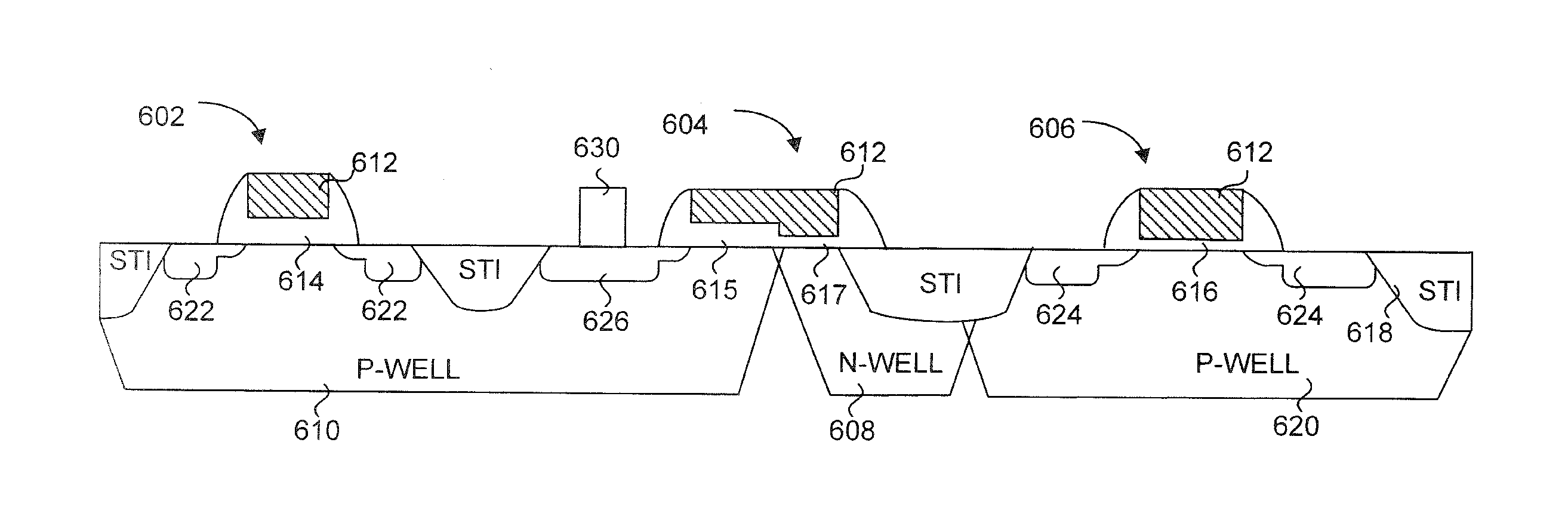
[0043]The embodiments of the present invention address the need for improved control of the dielectric breakdown of the anti-fuse device of OTP memory cells during the programming of the OTP cells, while minimizing current leakage. According to the present embodiments, this is achieved by fabricating the access transistor and anti-fuse device over wells of different or opposite type. Referred to as a twin well anti-fuse memory cell from this point forward, the present embodiments describe both single transistor 1T and two-transistor 2T memory cells using standard CMOS device processing without the need for added processing steps, since the structures of the twin well anti-fuse memory cells can be fabricated at the same time as the other transistor devices outside of the memory array are formed.

[0044]In particular, the twin well anti-fuse memory cells of the present embodiments comprise of a first well of a first type, a second well of the second type, an anti-fuse device formed over...


PUM


Abstract

A one time programmable memory cell having twin wells to improve dielectric breakdown while minimizing current leakage. The memory cell is manufactured using a standard CMOS process used for core and I/O (input/output) circuitry. A two transistor memory cell having an access transistor and an anti-fuse device, or a single transistor memory cell 100 having a dual thickness gate oxide 114&116, are formed in twin wells 102&104. The twin wells are opposite in type to each other, where one can be an N-type well 102 while the other can be a P-type well 104. The anti-fuse device is formed with a thin gate oxide and in a well similar to that used for the core circuitry. The access transistor is formed with a thick gate oxide and in a well similar to that used for I/O circuitry.

Description

CROSS REFERENCE TO RELATED APPLICATIONS[0001]This application claims the benefit of priority of U.S. Provisional Patent Application No. 61 / 256,608, filed on Oct. 30, 2009, the contents of which is incorporated herein by reference in its entirety.FIELD OF THE INVENTION[0002]The present invention relates generally to non-volatile memory. More particularly, the present invention relates to anti-fuse devices.BACKGROUND OF THE INVENTION[0003]In the following description the term MOS is used to denote any FET or MIS transistor, half-transistor or capacitor structure. In order to simplify the description of the embodiments, references to gate oxides from this point forward should be understood to include dielectric materials, oxide, or a combination of oxide and dielectric materials.[0004]Over the past 30 years, anti-fuse technology has attracted significant attention of many inventors, IC designers and manufacturers. An anti-fuse is a structure alterable to a conductive state, or in other...

Claims


Application Information

Patent Timeline
Patent Type & Authority Applications(United States)
IPC IPC(8): H01L27/092
CPCG11C17/16H01L27/11206H01L27/112H10B20/20H10B20/00
Inventor KURJANOWICZ, WLODEK
Owner SYNOPSYS INC
Why Eureka
Try Eureka