Method for forming metal thin film, semiconductor device and manufacturing method thereof

Inactive Publication Date: 2012-08-23
TOKYO ELECTRON LTD
View PDF7 Cites 3 Cited by
  • Summary
  • Abstract
  • Description
  • Claims
  • Application Information

AI Technical Summary

Benefits of technology

[0005]In view of the above, the present invention provides a method for forming a metal thin film as a single layer which functions as a Cu diffusion barrier film and a pla

Problems solved by technology

Further, the volume of the total film thickness is increased, thereby hindering the miniaturization of wiring patterns.
Moreover, when the cobalt film is formed as the plating seed layer, stress migration or electromigration develops due to poor wettability to Cu.
In addition, a delamination void is generated at the boundary between the Cu wiring and the Co seed layer, and defects such as disconnection and the like may occur.

Method used


Image

  • Method for forming metal thin film, semiconductor device and manufacturing method thereof
  • Method for forming metal thin film, semiconductor device and manufacturing method thereof
  • Method for forming metal thin film, semiconductor device and manufacturing method thereof

Examples


first embodiment

[0023]

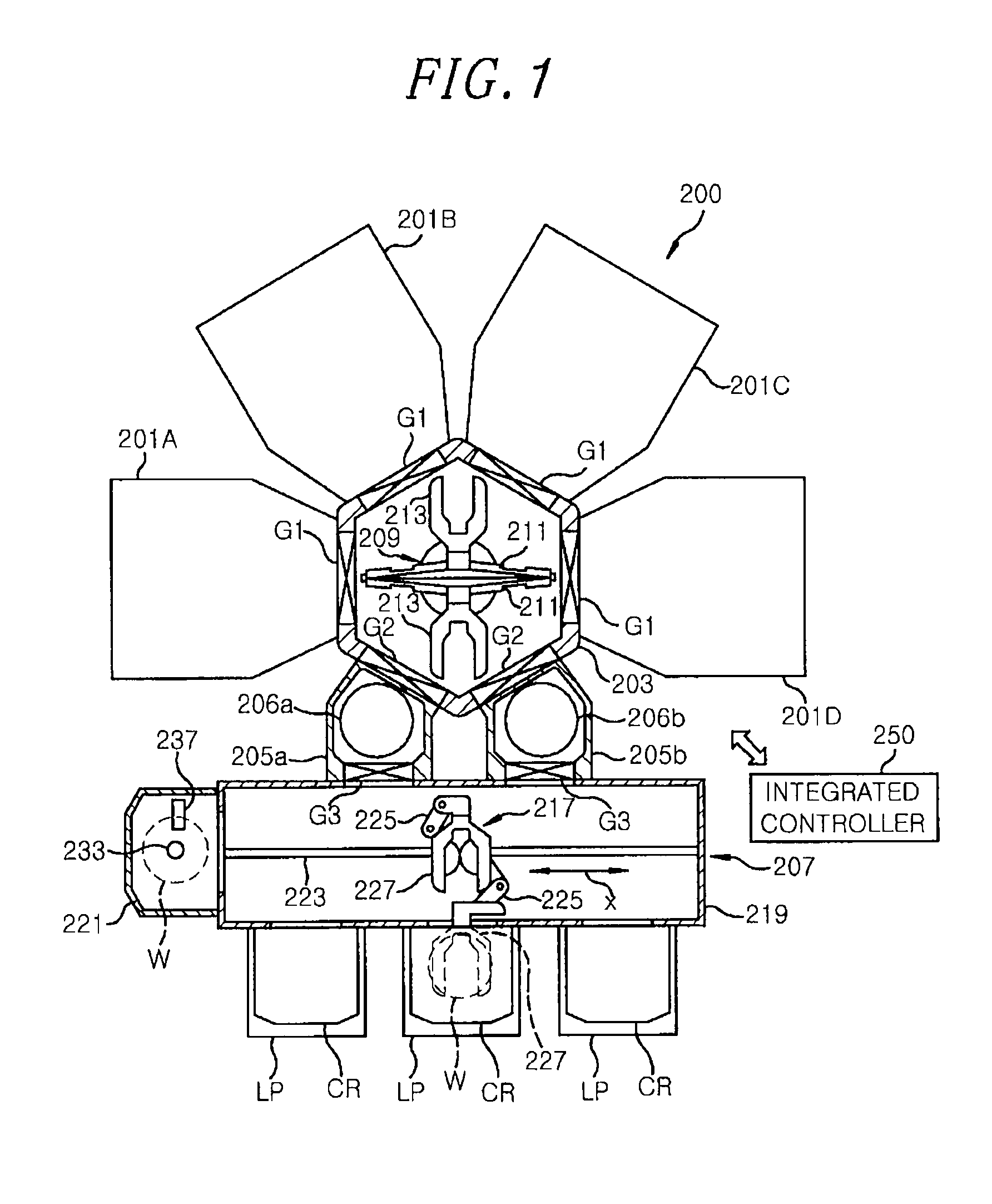
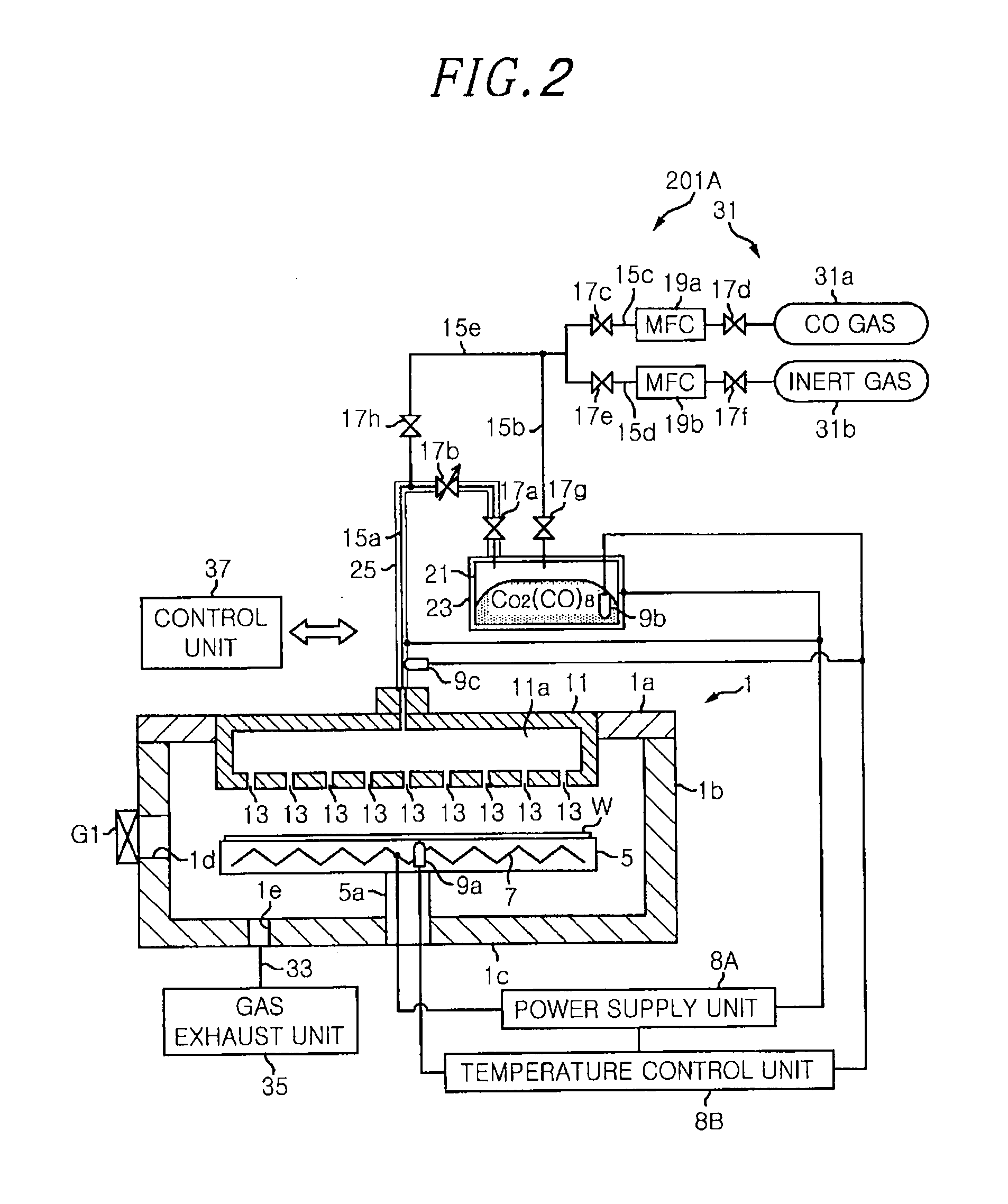
[0024]First, a configuration of a film forming apparatus suitable for performing a film forming method of the present invention will be described. First, a processing system which can be used in the present embodiment will be described with reference to FIG. 1. FIG. 1 is a schematic configuration view showing a processing system 200 configured to perform a process for forming a thin film containing Co2Ti alloy on a substrate, e.g., a semiconductor wafer (hereinafter, simply referred to as a “wafer”).

[0025]The processing system 200 shown in FIG. 1 is configured as a cluster tool of a multi-chamber structure including a plurality of (four in FIG. 1) process modules 201A to 201D. The processing system 200 mainly includes the four process modules 201A to 201D, a vacuum side transfer chamber 203 connected to the process modules 201A to 201D via gate valves G1, two load-lock chambers 205a and 205b connected to the vacuum side transfer chamber 203 via gate valves G2, and a loader uni...

second embodiment

[0128]A film forming method in accordance with a second embodiment of the present invention will be described.

[0129]FIG. 7 is a flowchart showing an example of a sequence of the film forming method of the present embodiment. FIG. 8 is a schematic cross sectional view showing a film forming apparatus 201E which can be used for the film forming method of the present embodiment. FIG. 9 is a reference view for explaining main processes of the film forming method of the present embodiment.

[0130]

[0131]The film forming apparatus 201E shown in FIG. 8 has the same configuration as that of the film forming apparatus (process module 201A) shown in FIG. 2 except the following features. Hereinafter, only the differences will be described, and like reference numerals will designate like parts of the film forming apparatus (process module 201A) shown in FIG. 2. The film forming apparatus 201E includes a shower head 12 connected to gas supply lines 15a and 15f. The shower head 12 for introducing a ...


PUM

PropertyMeasurementUnit
Thicknessaaaaaaaaaa
Ratioaaaaaaaaaa

Abstract

A metal thin film forming method includes depositing a Ti film on an insulating film formed on a substrate and depositing a Co film on the Ti film. The film forming method further includes modifying a laminated film of the Ti film and the Co film on the insulating film to a metal thin film containing Co3Ti alloy by heating the laminated film in an inert gas atmosphere or a reduction gas atmosphere.

Description

FIELD OF THE INVENTION[0001]The present invention relates to a method for forming a metal thin film, a semiconductor device having the metal thin film, and a manufacturing method thereof.BACKGROUND OF THE INVENTION[0002]In an LSI or an MEMS, although Cu has been conventionally used as a Cu plating seed layer for Cu wiring, studies have been made to use a cobalt film instead of the Cu film in order to improve embedding characteristics. When a cobalt film is used as a plating seed layer, it is expected that the adhesivity to a barrier film made of Ta, TaN or the like can be increased and the reliability of the Cu wiring can be improved (e.g., Japanese Patent Application Publication No. 2006-328526).[0003]The demand for high integration of semiconductor devices and scaling-down of chip sizes accelerates the miniaturization of wiring patterns. When the cobalt film is only used as a single layer, the barrier property against the diffusion of Cu is low and, thus, a barrier film needs to b...

Claims


Application Information

Patent Timeline
IPC IPC(8): H01L23/532H01L21/768
CPCC23C16/14C23C16/16C23C16/56H01L21/28556H01L21/76843H01L21/76858H01L2924/0002H01L21/76873H01L23/53238H01L2924/00
Inventor AZUMO, SHUJIKOJIMA, YASUHIKO
Owner TOKYO ELECTRON LTD
Why Eureka
Try Eureka