Film forming method and processing system

a technology of film forming and processing system, which is applied in the direction of coatings, vacuum evaporation coatings, basic electric elements, etc., can solve the problems of inferiority between the cu film and poor wetting property of the cu poor adhesion of the cu film to the mn film or the mn barrier film, etc., to achieve good barrier property and good adhesion

Active Publication Date: 2011-07-07
TOKYO ELECTRON LTD
View PDF8 Cites 21 Cited by
  • Summary
  • Abstract
  • Description
  • Claims
  • Application Information

AI Technical Summary

Benefits of technology

[0014]In view of the above, the present invention provides a film-forming method and a processing system, for forming a layer s

Problems solved by technology

In the meantime, the Mn barrier film has a relatively good barrier property against the Cu film, while the Cu film formed on the Mn film or the Mn barrier film has a relatively poor wetting property (wettabi

Method used


Image

  • Film forming method and processing system
  • Film forming method and processing system
  • Film forming method and processing system

Examples


second embodiment

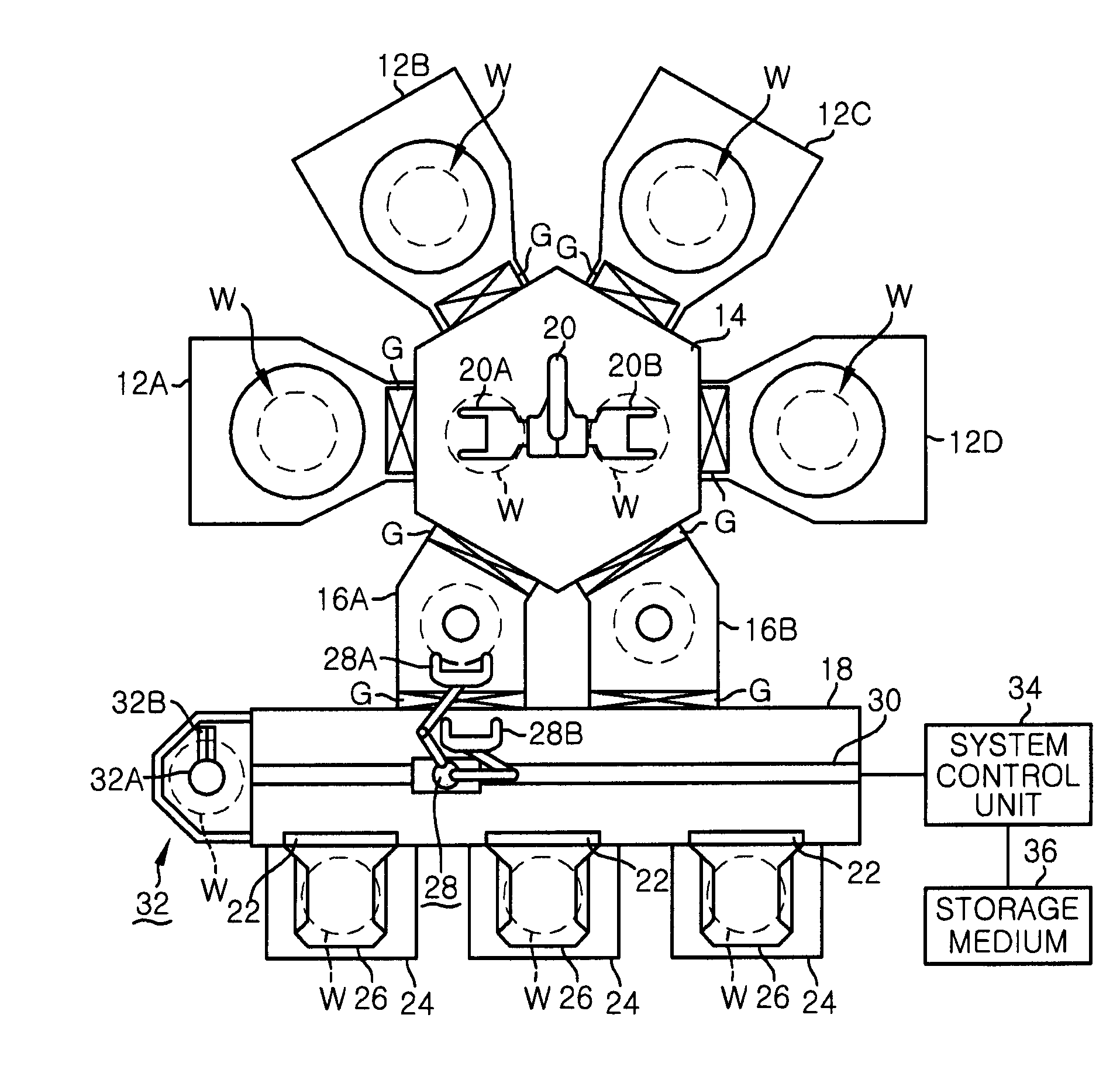
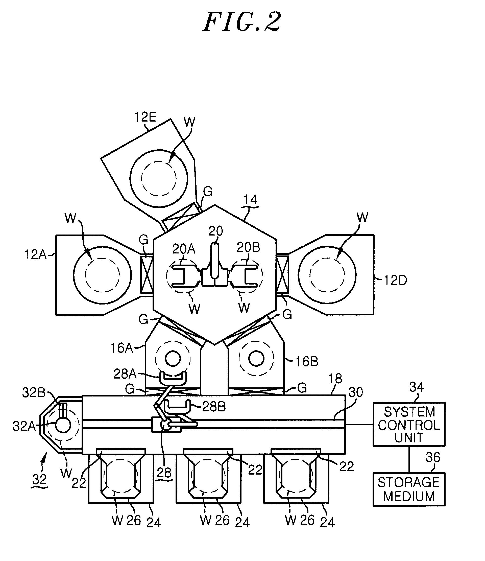
[0050]First, a processing system for performing the film-forming method of the present invention will be described. FIGS. 1 and 2 are schematic views respectively showing processing systems in accordance with a first and the present invention.

first embodiment

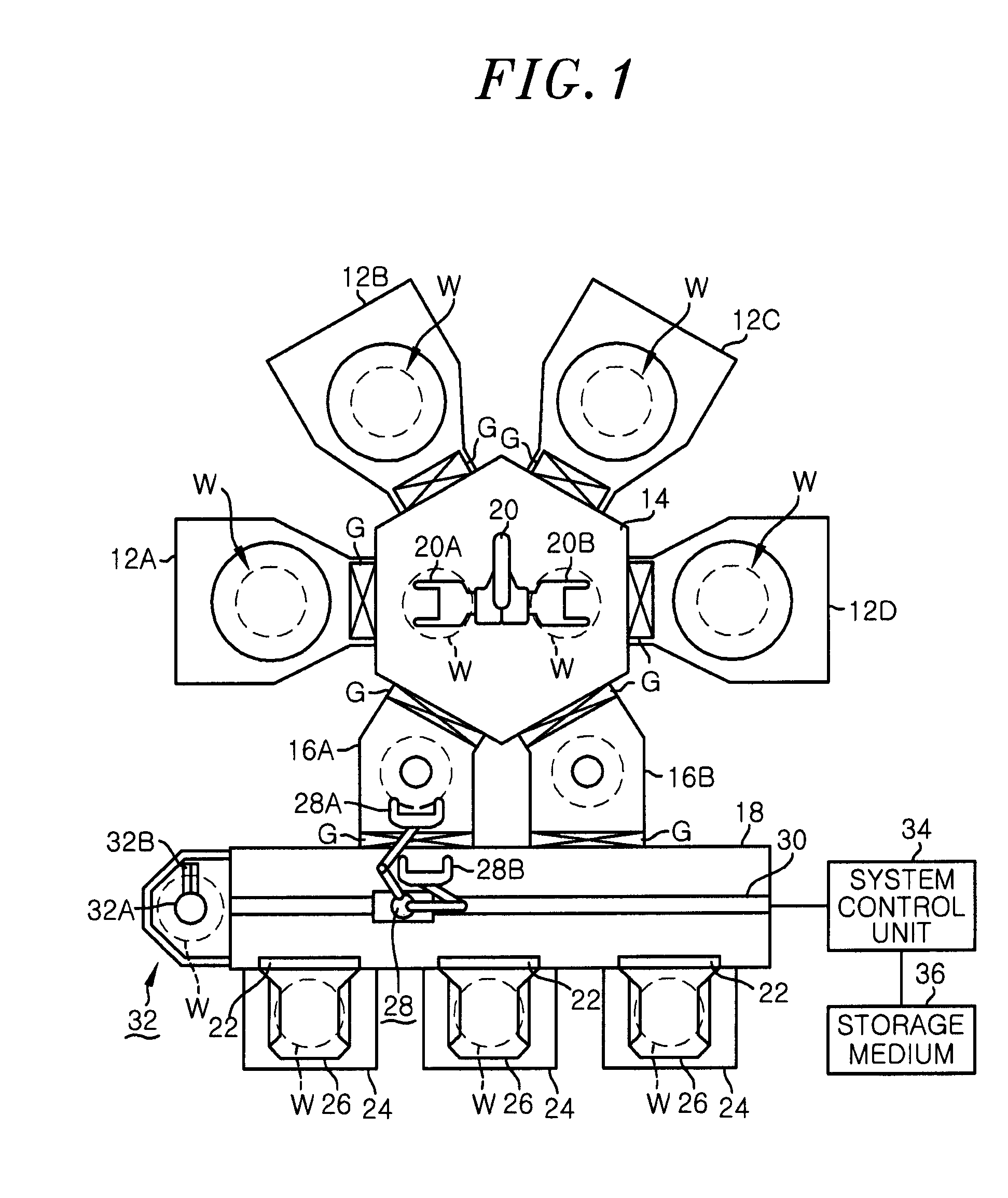
[0051]Hereinafter, the first embodiment will be described. As shown in FIG. 1, a processing system 10 mainly includes a plurality of, e.g., four processing apparatuses 12A to 12D; an approximately hexagonal common transfer chamber 14; a first and a second load-lock chamber 16A and 16B having a load-lock function; and an inlet side transfer chamber 18 extended longitudinally.

[0052]In this embodiment, one (e.g., the processing apparatus 12A) of the four processing apparatuses 12A to 12D serves to perform a pre-treatment on a target substrate, e.g., a semiconductor wafer W, to be processed. Another one (e.g., the processing apparatus 12B) of the four processing apparatuses 12A to 12D serves to form a film containing a transition metal on the semiconductor wafer W. Still another one (e.g., the processing apparatus 12C) of the four processing apparatuses 12A to 12D serves to form a metal film containing an element of the group VIII of the periodic table on the semiconductor wafer W. The ...


PUM

PropertyMeasurementUnit
Structureaaaaaaaaaa

Abstract

Provided is a film-forming method for performing a film-forming process on a surface of a target substrate to be processed in an evacuable processing chamber, a recessed portion being formed on the surface of the target substrate. The method includes a transition metal-containing film processing process in which a transition metal-containing film is formed by a heat treatment by using a source gas containing a transition metal; and a metal film forming process in which a metal film containing an element of the group VIII of the periodic table is formed.

Description

[0001]This application is a Continuation Application of PCT International Application No. PCT / JP2009 / 062380 filed on Jul. 7, 2009, which designated the United States.FIELD OF THE INVENTION[0002]The present invention relates to a film-forming method and a processing system, for forming, e.g., a film containing manganese and a film containing ruthenium serving as barrier layers on a surface of a target substrate, e.g., a semiconductor wafer, to be processed.BACKGROUND OF THE INVENTION[0003]In general, processes such as a film-forming process and a pattern etching process are repeatedly performed to manufacture semiconductor devices. In this regard, the line width and hole diameter become gradually reduced in response to the demand for higher integration and higher miniaturization of the semiconductor devices. Since it is required to reduce the electric resistance further due to the scaling-down of various dimensions, an inexpensive copper having a small electric resistance tends to be...

Claims


Application Information

Patent Timeline
IPC IPC(8): H01L23/532B05C11/00H01L21/768
CPCC23C16/045C23C16/18H01L2924/0002C23C16/40C23C16/45523H01L21/02063H01L21/28556H01L21/76814H01L21/76831H01L21/76846H01L21/76873H01L23/53238H01L2924/09701H01L2924/00H01L21/285H01L21/3205C23C14/14
Inventor MATSUMOTO, KENJIMIZUSAWA, YASUSHI
Owner TOKYO ELECTRON LTD
Why Eureka
Try Eureka