Mode Latching Buffer Circuit

Active Publication Date: 2012-08-23
AVAGO TECH INT SALES PTE LTD
View PDF5 Cites 13 Cited by
  • Summary
  • Abstract
  • Description
  • Claims
  • Application Information

AI Technical Summary

Benefits of technology

[0006]Principles of the invention, in illustrative embodiments thereof, advantageously provide a buffer circuit architecture that provides full functional modes even when a core voltage supply to the buffer circuit is powered down (i.e., turned off). Moreover, the buffer circuit architecture, according to aspects of the invention, is able to provide such full functional modes using a single control signal. In this manner, the buffer circuit according to embodiments of the invention can advantageously offer a full set of functional modes even when the core voltage supply to the buffer circuit is turned off (or otherwise disconnected) without increasing design complexity, layout routing congestion, or other problems associated with conventional approaches.

Problems solved by technology

However, with smaller feature sizes (e.g., gate oxide thickness, gate channel width and length, etc.) in current technologies, there is a significant amount of leakage current (e.g., sub-threshold leakage current) even when a functional block is powered off.
This approach, however, increases layout routing congestion and design complexity, among other disadvantages.
However, a full set of modes that an I / O buffer may offer during normal operation is not realizable when the core power supply to the buffer circuit is removed (i.e., turned off or otherwise disconnected).
Given the number and complexity of current I / O buffers employed in a given SoC design, however, it is simply impractical to provide as many I / O level signals as there are core level signals.
This approach also increases design complexity, layout routing congestion, and characterization, verification and functional model complexities, and is therefore undesirable.

Method used


Image

  • Mode Latching Buffer Circuit
  • Mode Latching Buffer Circuit
  • Mode Latching Buffer Circuit

Examples


Embodiment Construction

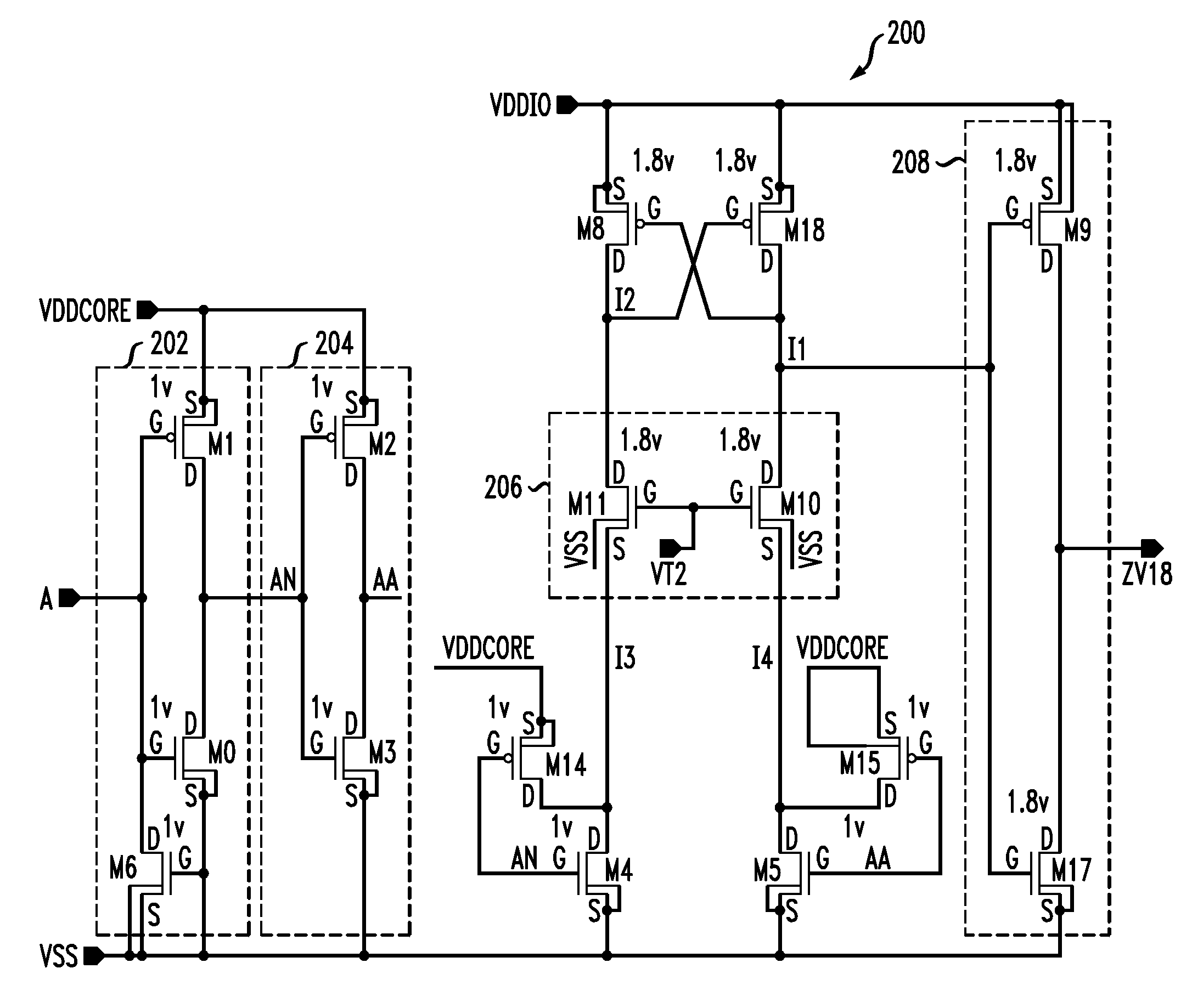
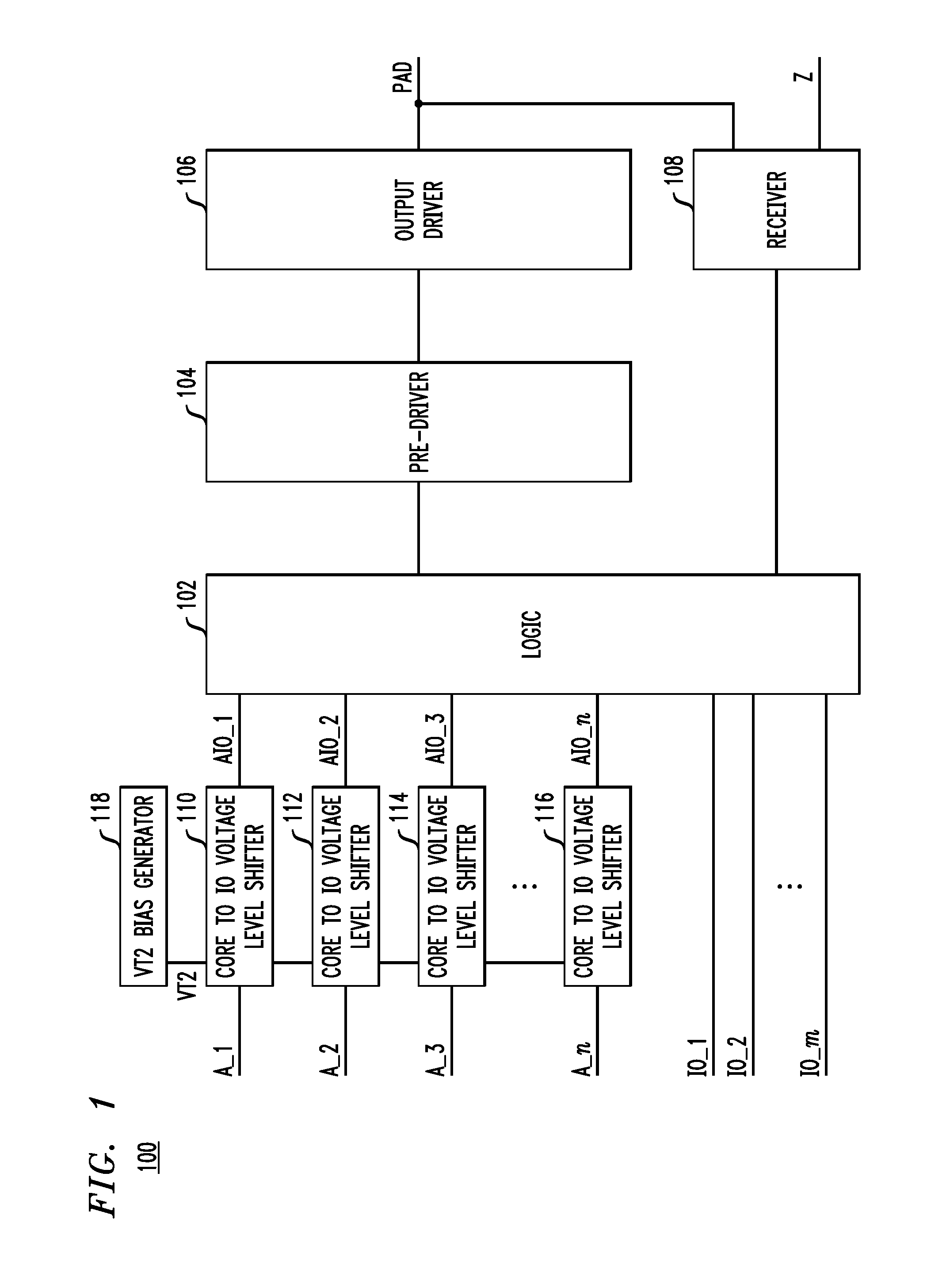
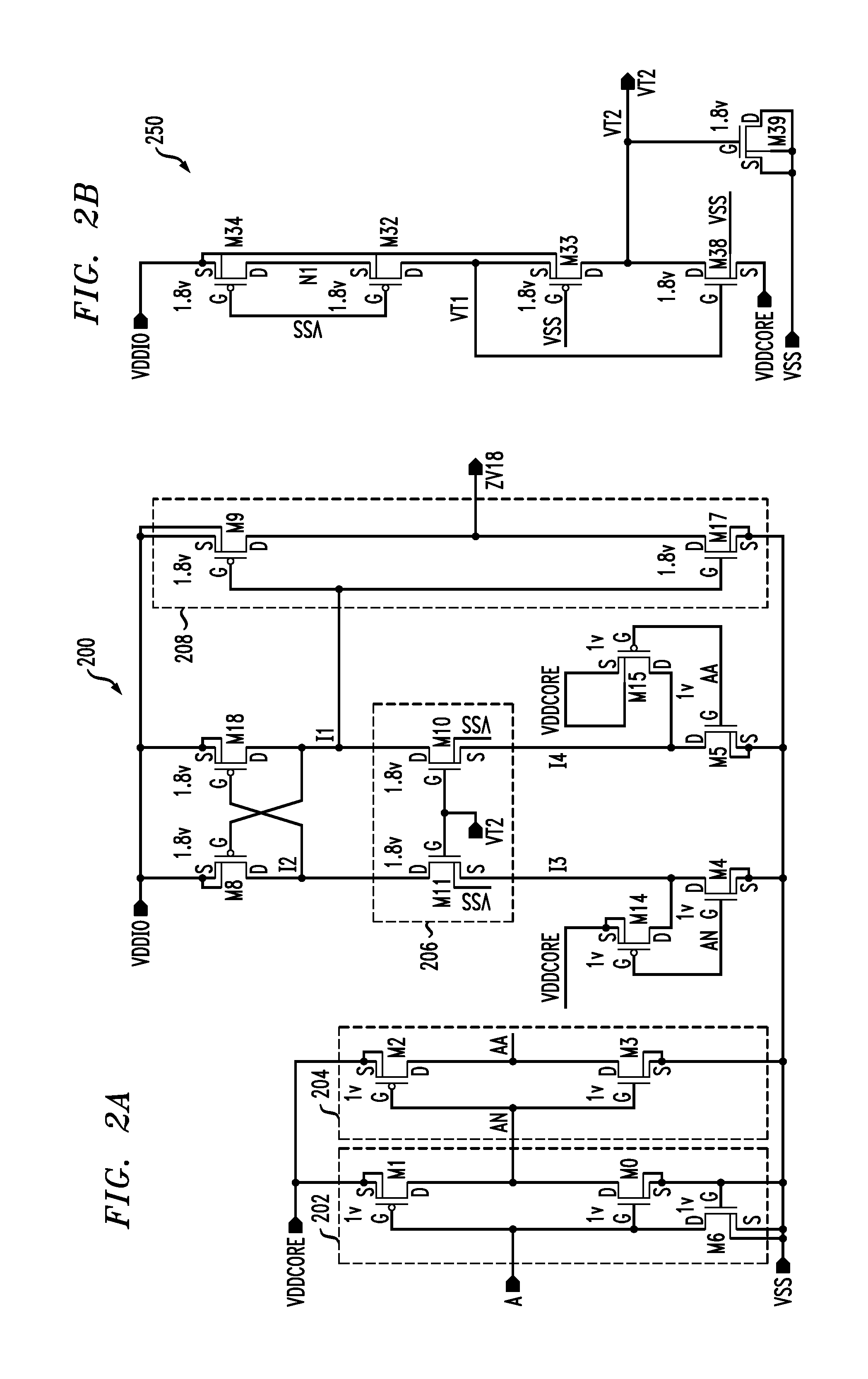
[0018]Principles of the present invention will be described herein in the context of illustrative I / O buffer circuits and voltage translator circuits. It should be understood, however, that the present invention is not limited to these or any other particular circuit arrangements. Rather, embodiments of the invention are more generally applicable to a buffer circuit architecture which offers full functional modes of the buffer circuit even when a core voltage supply to the buffer circuit is powered down or otherwise disconnected from the buffer circuit. A buffer circuit according to aspects of the invention is able to provide full functional modes when the core voltage supply is powered down using a substantially reduced set of control signals, thereby beneficially eliminating various disadvantages of standard approaches, including, but not limited to, layout routing congestion and design complexity. Moreover, it will become apparent to those skilled in the art given the teachings h...


PUM


Abstract

A voltage translator circuit includes an input stage adapted for receiving an input signal referenced to a first voltage supply, a first latch circuit adapted for connection with a second voltage supply and operative to at least temporarily store a logic state of the input signal, and a voltage clamp coupled between the input stage and the first latch circuit. The voltage clamp is operative to set a maximum voltage across the input stage to a prescribed level. The voltage translator circuit generates a first output signal at a first output formed at a junction between the first latch circuit and the voltage clamp. A second latch circuit is connected to the first output in a feedback configuration. The second latch circuit is operative to retain a logical state of the first output signal as a function of at least a first control signal supplied to the second latch circuit regardless of a state of the first voltage supply.

Description

FIELD OF THE INVENTION[0001]The present invention relates generally to electrical and electronic circuitry, and more particularly relates to buffer circuits.BACKGROUND OF THE INVENTION[0002]In order to reduce costs and time to market, current integrated circuit (IC) designs often incorporate several functionalities into a single chip. This is particularly true as IC fabrication technologies move towards ultra-deep sub-micron geometries, such as, for example, 40 nanometer (nm) or 28 nm. Such a design approach is typically referred to as a system on a chip (SoC).[0003]In order to conserve power in a SoC design, it is important that different functional blocks in the SoC be capable of being independently turned off (i.e., powered down) when they are inactive. However, with smaller feature sizes (e.g., gate oxide thickness, gate channel width and length, etc.) in current technologies, there is a significant amount of leakage current (e.g., sub-threshold leakage current) even when a func...

Claims


Application Information

Patent Timeline
IPC IPC(8): H03K19/0175H03K5/08
CPCH03K19/018521H03K3/356182
Inventor NICHOLAS, PETER J.KRIZ, JOHN CHRISTOPHERBHATTACHARYA, DIPANKARBRADLEY, JAMES JOHN
Owner AVAGO TECH INT SALES PTE LTD
Why Eureka
Try Eureka