Tracking analog-to-digital converter (ADC) with a self-controlled variable clock

a technology of analog-to-digital converter and self-controlled variable clock, which is applied in the direction of analog-to-digital converters, instruments, transmission systems, etc., can solve the problems of difficult design of such a device, relatively short settling time, and relatively long settling time, and achieve significant speed increase, low power consumption, and speed of tracking adc

Inactive Publication Date: 2012-08-23
DIALOG SEMICONDUCTOR GMBH
View PDF1 Cites 19 Cited by
  • Summary
  • Abstract
  • Description
  • Claims
  • Application Information

AI Technical Summary

Benefits of technology

[0012]The settling time that a comparator requires to compare the signals is not constant. Rather, the comparator settling time varies greatly depending on the difference between the input and the feedback signal, where the settling time is at its maximum when the difference between the input signal and the D / A-converted feedback signal from the digital register is at its minimum. This maximum settling time corresponds to small input differences on the order of one LSB. In contrast, the settling time when the difference is large is substantially shorter. Thus, the settling time is relatively short when the input signal changes significantly in magnitude, and the settling time is relatively long when the signal changes are small.
[0013]The tracking ADC described in this application is based on this characteristic by configuring the device to take advantage of the fact that the settling time of the comparator is relatively short when the difference between the input signal and the D / A converted output feedback signal is large, which also corresponds to the conditions under which slewing occurs. Thus, the tracking ADC described in this application solves the above problems by providing a tracking ADC that can be driven with a self-controlled variable clock based on a determination of the settling time of the comparator. Therefore, the maximum clock rate of this design is primarily limited by the settling time of comparator, allowing the clock rate to be substantially increased in response to large input changes, further allowing the slewing time to be thereby greatly reduced.
[0014]Thus, the tracking ADC described in this application provides shorter tracking times in response to large input changes such as a step in the input. Additionally, this possibility to increase the clock rate allows the tracking ADC to better operate with a self-controlled variable clock to provide high speed analog-to-digital conversion by reducing slewing, thereby allowing for fast tracking of large input changes. The proposed tracking ADC further has a low error rate and low power requirements without requiring complex additional correction hardware.

Problems solved by technology

The design of a device that achieves all these competing goals in combination makes the design of such a device challenging.
Thus, the settling time is relatively short when the input signal changes significantly in magnitude, and the settling time is relatively long when the signal changes are small.
In particular, the primary disadvantage of tracking ADCs relating to the slewing of the digital output at large input signal steps can be improved by dynamically increasing the clock rate during the time period when the digital output is slewing.
When the tracking ADC is clocked with a self-controlled variable clock, the clock rate is typically limited by the settling time of the comparator and the settling time of the feedback DAC as well as some additional time for the digital control logic.
Thus, particularly during heavy slewing, where although the settling time of the comparator is very short, the use of a fixed rate clock that must take the maximum settling time into account makes it difficult for the ADC to track large input changes quickly.
Thus, during the time that the comparator is determined to not be ready, the output of the comparator is not reliable and generally should not be read (unless special hold or latch output elements are used).
When the tracking ADC is clocked with a self-controlled variable clock, the clock rate is typically limited by the settling time of the comparator and the settling time of the feedback DAC as well as some additional time for the digital control logic.
In addition, the time necessary to reset the comparator may also limit the maximum clock rate.
In particular, if the next clock cycle begins before internal signals and the outputs of the comparator have time to be properly reset, transient output signals may be produced or an output signal even may be missed entirely.
Furthermore, insufficient reset time may result in incomplete reset of the voltages of the latch stage, resulting in hysteresis of the comparator.
Thus, with a tracking ADC is clocked with a self-controlled variable clock under heavy slewing, the maximum clock rate may be primarily limited by the settling time of the feedback DAC and the time for the digital control logic.
For example, during heavy slewing when the settling time of the comparator is very short, the slewing of the thermometer coded DAC and the delay of the logic may become dominant.
However, monotonous output is most important for step changes of one single LSB.
In particular, the maximum clock rate of the tracking ADC described in this application is primarily limited by reset time and settling time of comparator, which can be further reduced through the appropriate choice of components.

Method used


Image

  • Tracking analog-to-digital converter (ADC) with a self-controlled variable clock
  • Tracking analog-to-digital converter (ADC) with a self-controlled variable clock
  • Tracking analog-to-digital converter (ADC) with a self-controlled variable clock

Examples


Embodiment Construction

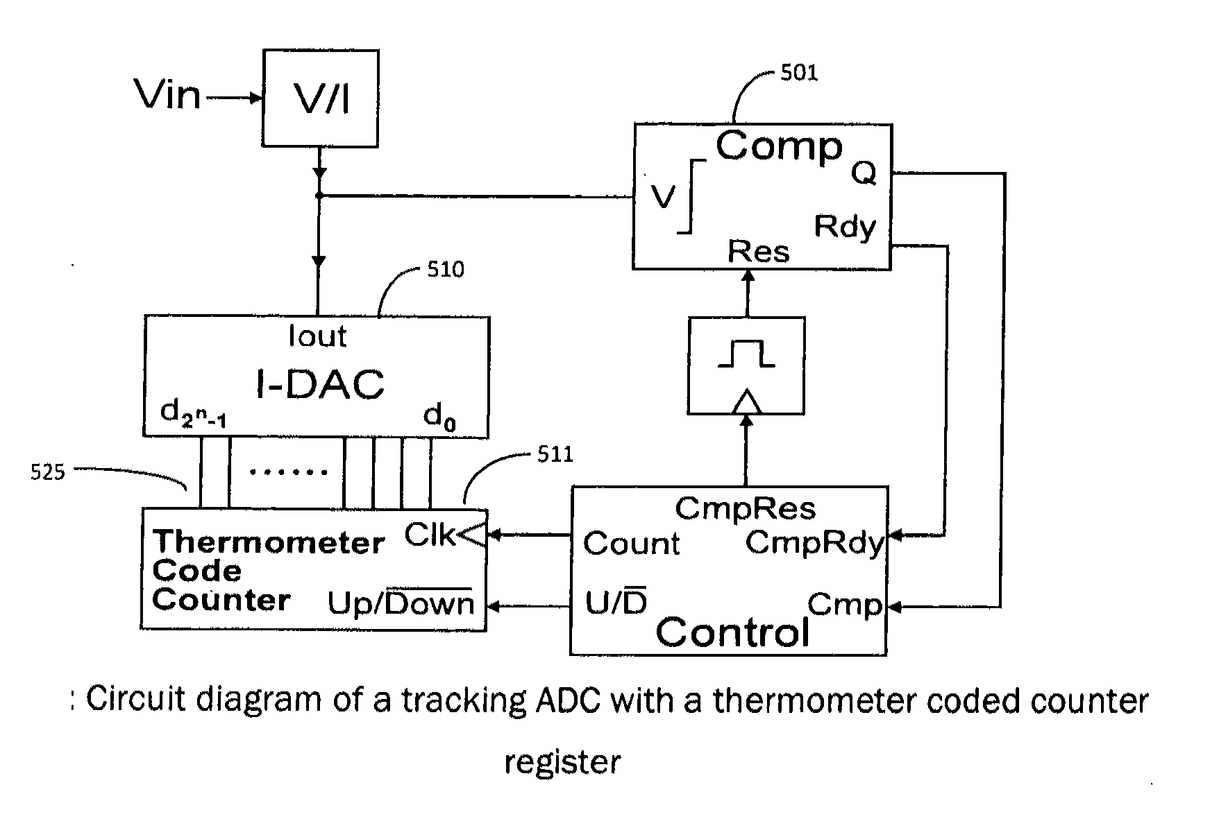
[0061]In general, an ADC based upon the comparison of the analog input and the D / A-converted output can be operated with currents, voltages or charges. If the comparison is done with currents, a positive and a negative current are added and converted to a voltage by the output impedance of the current sources, where one of the currents is derived from the analog input, and the other current is derived from the D / A-converted digital output. The voltage is then fed to the input of a comparator.

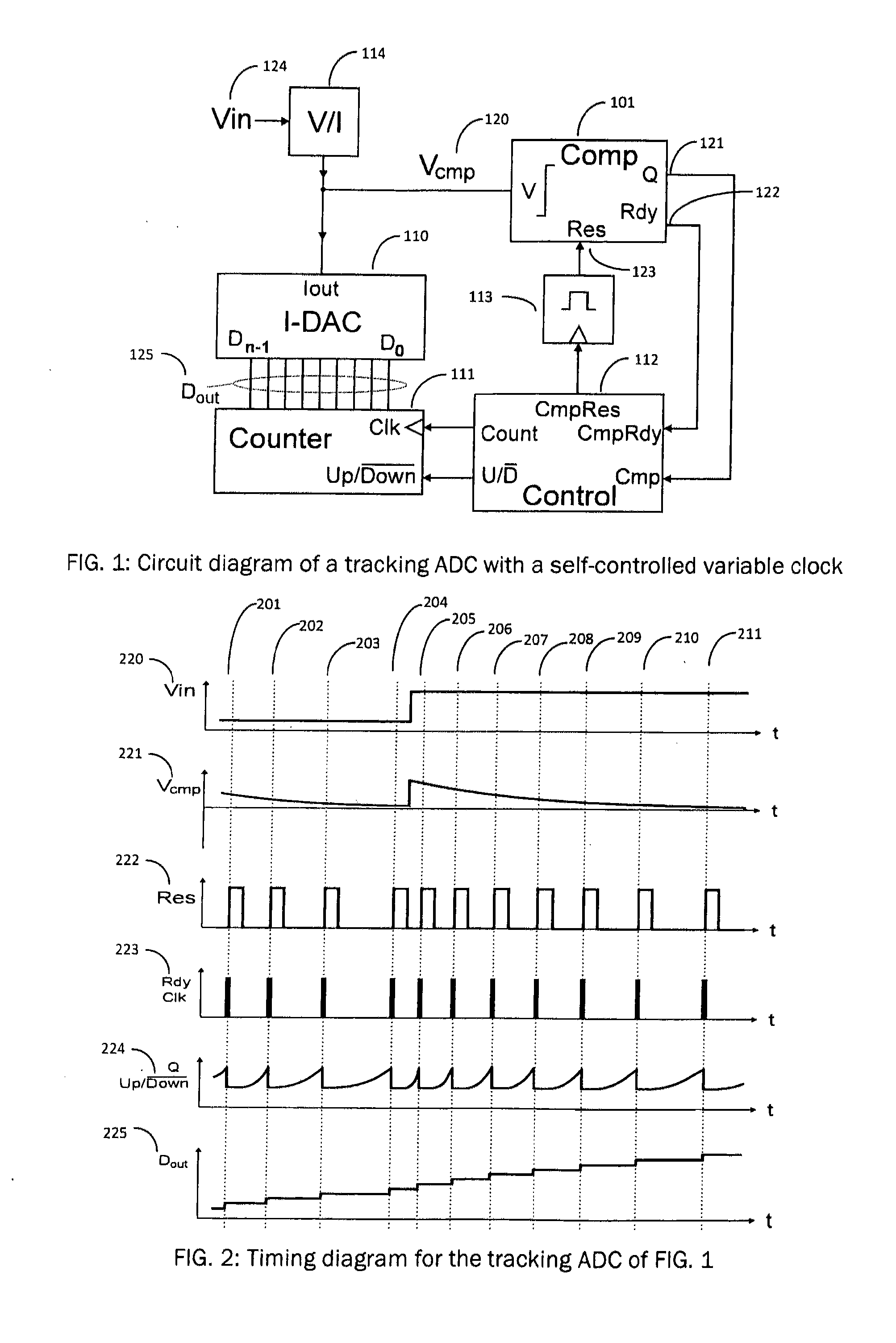
[0062]FIG. 1 shows a circuit diagram for a tracking ADC with a self-controlled variable clock according to a preferred embodiment of the present invention. The tracking ADC of FIG. 1 comprises an up-down counter 111, whose output signal is a digital counter signal Dout 125. This digital counter signal Dout 125 is fed into a DAC 110. In FIG. 1 the analog input voltage Vin 124 is converted to a current by component 114 (V / I-Converter, transconductance) and then compared with a current derived from...


PUM


Abstract

A tracking analog-to-digital converter “ADC” with a self-controlled variable clock comprises: a digital register; a digital-to-analog converter “DAC” coupled to said digital register providing an analog feedback signal; a comparator coupled to an analog input signal and said analog feedback signal and providing a comparison signal based on a comparison between said analog input signal and said analog feedback signal, said comparison signal being coupled to the digital register; a means for determining comparator readiness to determine if said comparator is ready, indicating that said comparison signal can be reliably read, said means for determining comparator readiness further comprising a determination of a comparison ready indicator; a means for clocking to generate a clock signal to drive said digital register in response to said means for determining comparator readiness determining that said comparator is ready; and said digital register being configured to count in response to said clock signal based on said comparison signal of the comparator.

Description

BACKGROUND OF THE INVENTION[0001](1) Field of the Invention[0002]This invention relates to conversion of analog signals to digital signals. In particular, it relates to a tracking analog-to-digital converter (ADC) providing analog-to-digital conversion.[0003](2) Description of the Prior Art[0004]In the computer and information age, digital technology continues to increase in importance. With advances in technology, more and more everyday devices now incorporate digital technology and operate with digital signals. However, many of the real signals that are controlled, sampled and measured by digital systems exist not as digital signals but as analog signals, which must first be converted from analog to digital form before they can be incorporated into a digital system. Thus, an important device in the implementation of both digital and analog systems is the analog-to-digital converter (ADC or A / D converter), which is a device that converts an analog input signal into a digital number...

Claims


Application Information

Patent Timeline
Patent Type & Authority Applications(United States)
IPC IPC(8): H03M1/12
CPCH03M1/1215H03M1/48H03M1/125
Inventor KILLAT, DIRKYAN, HUANG
Owner DIALOG SEMICONDUCTOR GMBH
Why Eureka
Try Eureka