Multi-chip module package
a module package and module technology, applied in the direction of semiconductor devices, electrical equipment, semiconductor/solid-state device details, etc., can solve the problems of adversely affecting the reliability of the package structure, the process for fabricating the package structure b>5/b> is complicated, and the fabricating cost is increased, so as to reduce the fabrication cost, and simplify the fabrication process
- Summary
- Abstract
- Description
- Claims
- Application Information
AI Technical Summary
Benefits of technology
Problems solved by technology
Method used
Image
Examples
first embodiment
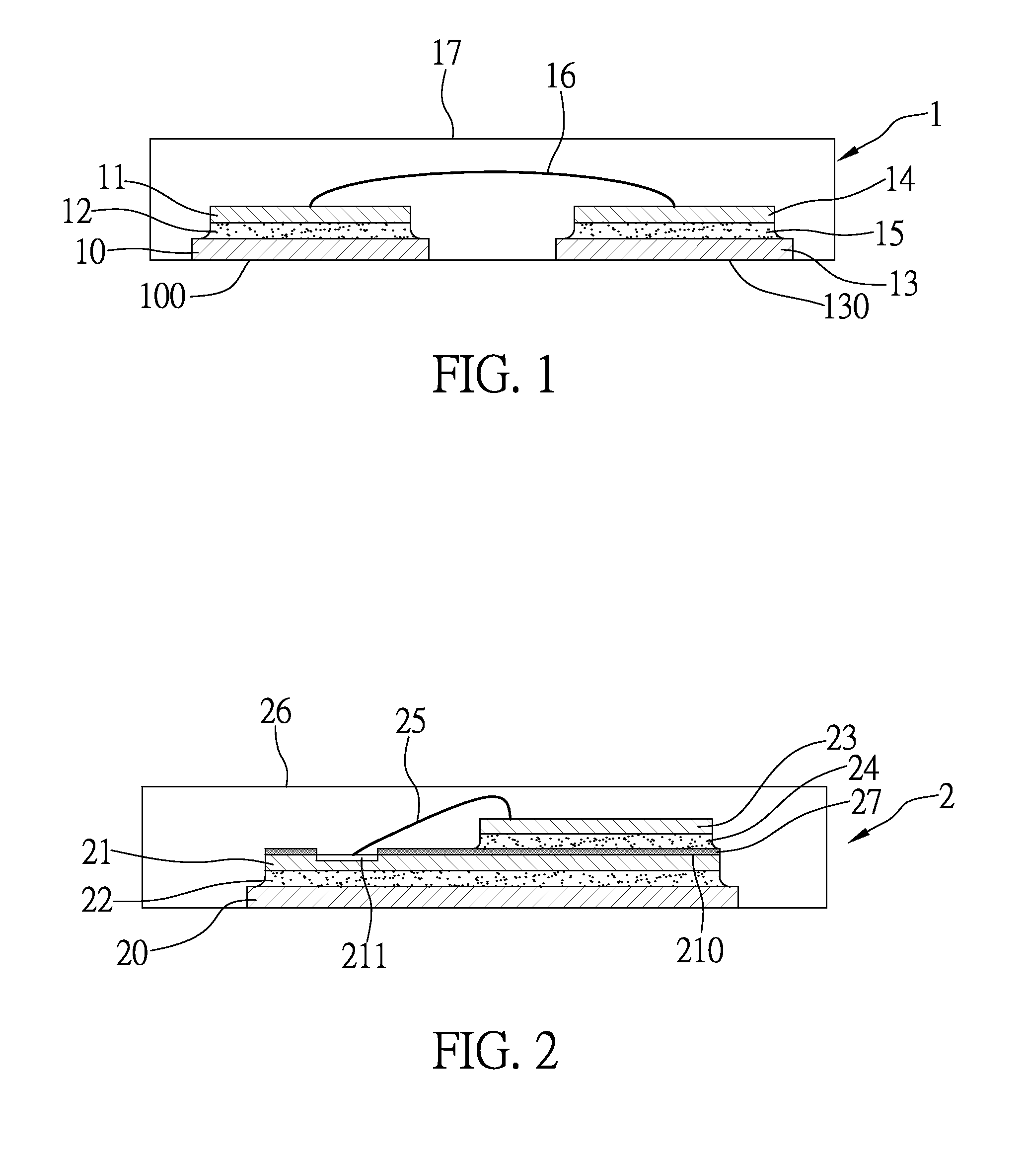
[0030]Referring to FIG. 1, a cross-sectional view of the multi-chip module package according to the first embodiment of the present invention is shown. As shown in the drawing, the multi-chip module package 1 is composed of a first die pad 10 of a lead frame (merely the die pad 10 of the lead frame is shown for the sake of simplification), a switching chip 11 mounted on via a first conductive adhesive 12 and electrically connected to the first die pad 10, a second die pad 13 of the lead frame (not shown) spaced apart from the first die pad 10 by a predetermined distance, a driving chip 14 mounted on via a second conductive adhesive 15 and electrically connected to the second die pad 13, a plurality of bonding wires 16 for electrically connecting the switching chip 11 to the driving chip 14, and an encapsulant 17 for encapsulating the first and second die pads 10 and 13, the switching chip 11, the driving chip 4, and the plurality of bonding wires 16, while allowing a bottom surface ...
second embodiment
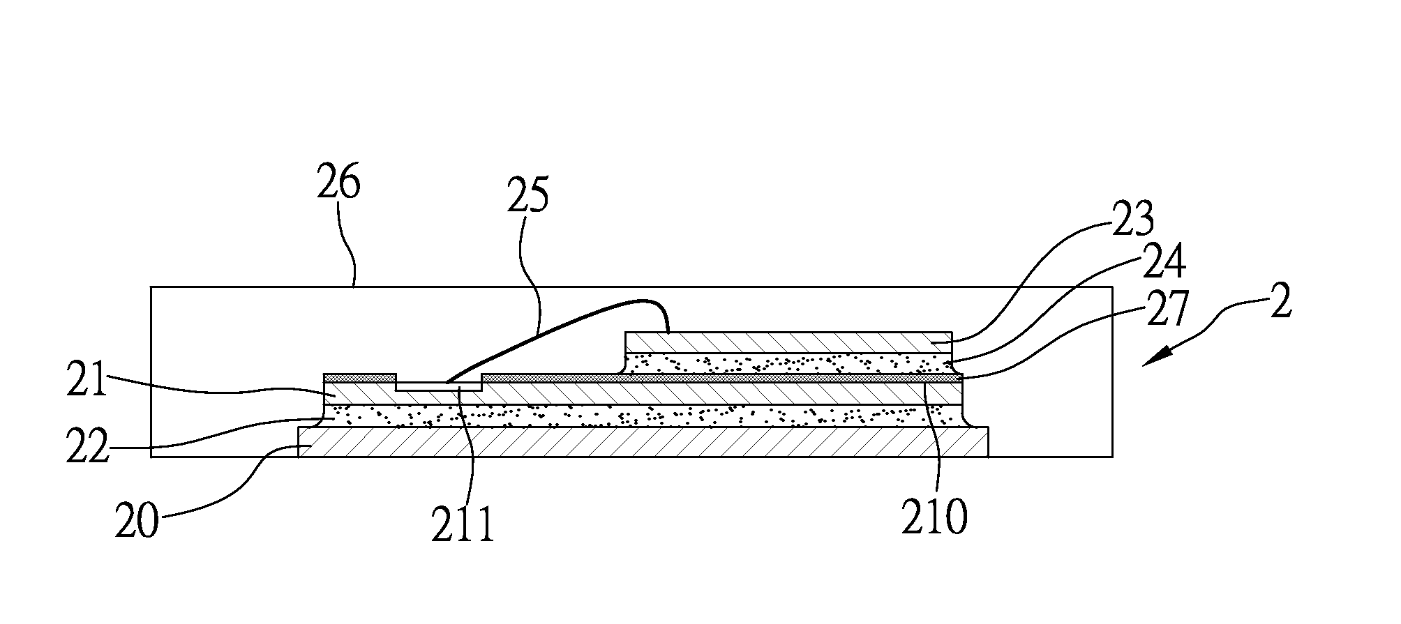
[0035]Referring to FIG. 2, a cross-sectional vies of a multi-chip module package according to the second embodiment of the present invention is shown.
[0036]As shown in the drawing, the multi-chip module package 2 of the second embodiment has a die pad 20 of a lead frame (not shown) for a switching chip 21 to be mounted thereon via a first conductive adhesive 22 and electrically connected thereto via a plurality of bonding wires (not shown). A driving chip 23 is then stacked on the switching chip 21 via a second conductive adhesive 24 and electrically connected to the switching chip 21 via a plurality of bonding wires 25. And, an encapsulant 26 is formed to encapsulate the die pad 20, the switching chip 21, the driving chip 23 and the bonding wires 25, but allowing a bottom surface (not shown) of the die pad 20 to be exposed from the encapsulant 26.
[0037]To secure the insulation of the switching chip 21 and the driving chip 23, on an active surface 210 of the switching chip 21 an ins...
third embodiment
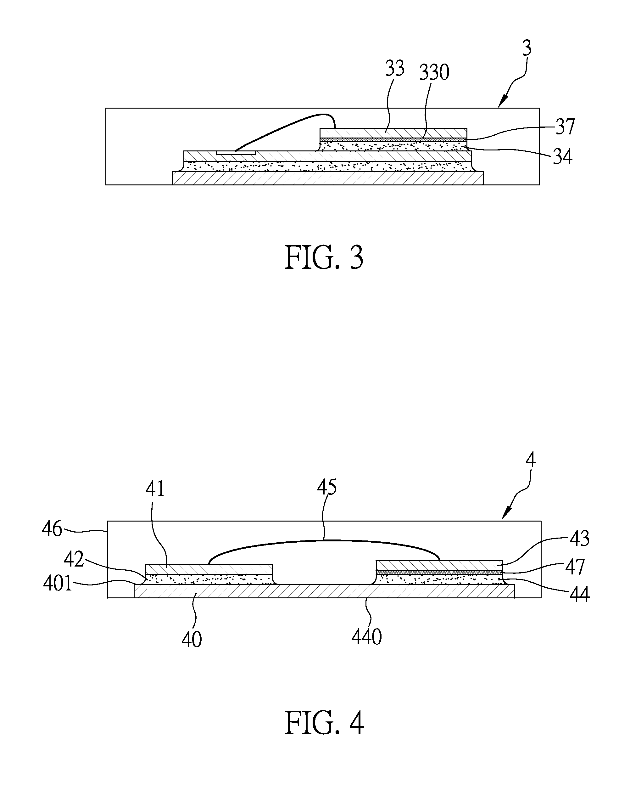
[0039]Referring to FIG. 3, a cross-sectional view of a multi-chip module package according to a third embodiment of the present invention is shown.
[0040]As shown in the drawing, the multi-chip module package 3 of the third embodiment of the present invention is essentially similar in structure to the package 2 of the second embodiment described above, except that an insulating layer 37 is formed on a non-active surface 330 of the driving chip 33, allowing the insulating layer 37 to be interposed between the second conductive adhesive 34 and the driving chip 33. The insulating layer 37 can be formed on a bottom surface of a wafer (not shown) for being sawed into individual driving chip 33 whereby there will be no additional formation process for the assembly of the multi-chip module package 3.
PUM
 Abstract
Description
Claims
Application Information


