PCB with heat dissipation structure and processing methods thereof

a heat dissipation structure and printed circuit board technology, applied in the direction of printed circuit aspects, dielectric characteristics, porous dielectrics, etc., can solve the problems of air being a poor heat conductor, heat dissipation, and relatively slow heat dissipation speed of the support plate, and achieve simple structure, low cost, and heat dissipation structure.

Inactive Publication Date: 2012-09-06
SHENZHEN CHINA STAR OPTOELECTRONICS TECH CO LTD
View PDF2 Cites 3 Cited by
  • Summary
  • Abstract
  • Description
  • Claims
  • Application Information

AI Technical Summary

Benefits of technology

[0005]The main object of the invention is to provide a PCB with a heat dissipating structure, which has simple structure, low cost and good heat dissipating effect. Simultaneously, the invention also provides a method for processing the PCB with a heat dissipating structure.

Problems solved by technology

However, the heat dissipating speed of the support plate is relatively slow, so that heat dissipation needs to be finished by means of other heat dissipating devices during the connection process of electrical appliances.
However, when a light bar on the PCB is arranged on other heat dissipating component, the LED cannot dissipate heat easily through the PCB and the heat dissipating component because a plurality of grooves or gaps exist between the PCB and the contact interface of the heat dissipating component, a very thin air layer is formed, the air is a poor heat conductor and the heat resistance is high.
However, the conventional methods have the defects of increase of working procedures, poor heat dissipating effect, complicated installation, higher cost and inconvenience for carrying and repairing.

Method used


Image

  • PCB with heat dissipation structure and processing methods thereof
  • PCB with heat dissipation structure and processing methods thereof
  • PCB with heat dissipation structure and processing methods thereof

Examples


Embodiment Construction

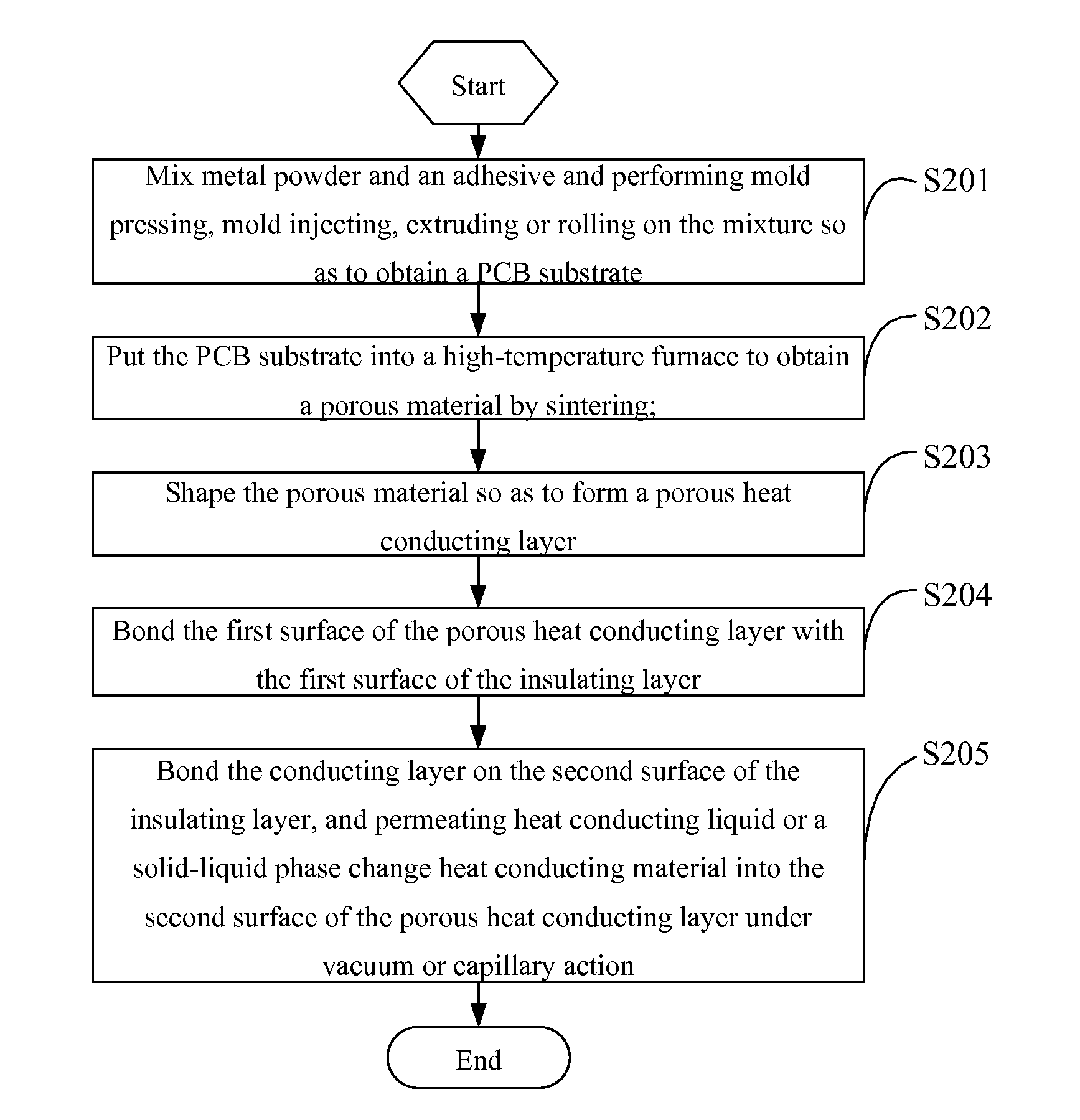
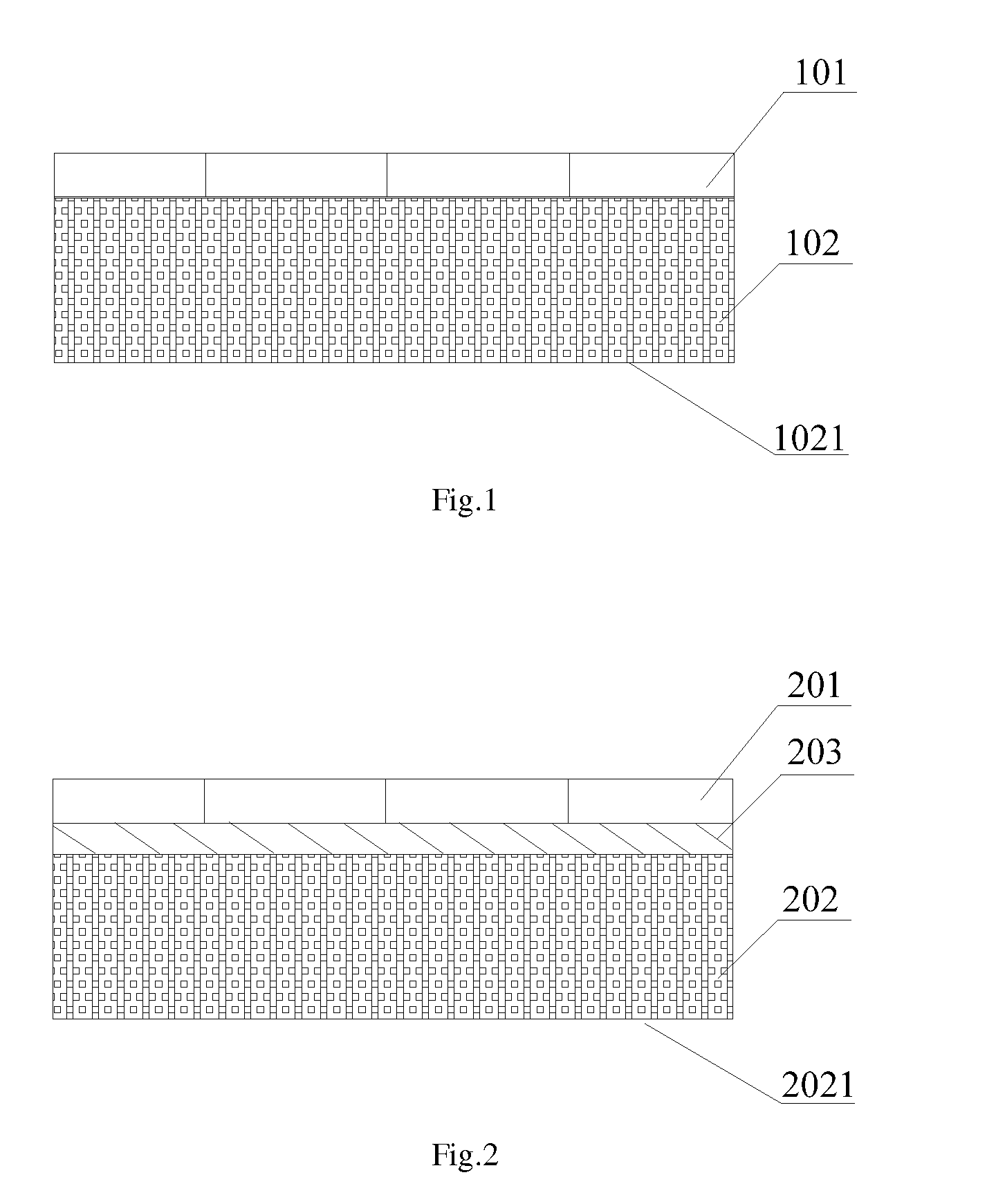
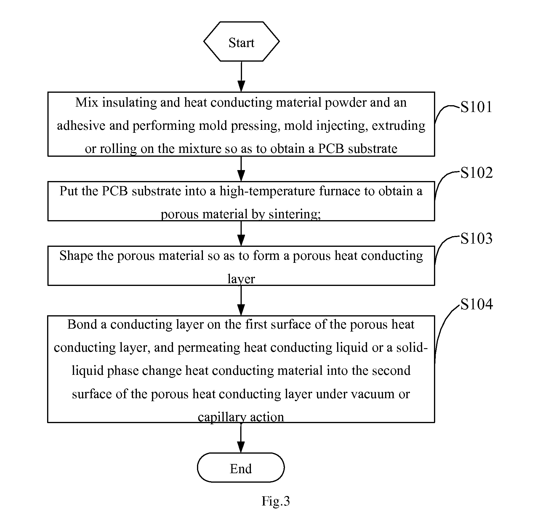
[0035]The general thought of the technical solution of the invention is: making the carrier layer of the PCB into a porous heat conducting layer with electric insulating and heat conducting functions or electric and heat conducting functions, and injecting heat conducting liquids such as heat conducting ink or a solid-liquid phase change heat conducting material into holes of the porous heat conducting layer, so as to reduce the heat resistance between the LED and the contact interface of the PCB and enhance the heat conducting effect of the PCB.

[0036]The technical solution for realizing the object of the invention is explained in detail in combination with attached drawings and embodiments in the following paragraphs. It should be understood that the embodiments described here are only used for explaining the invention but not limiting the patent scope of the invention.

[0037]By referring to FIG. 1, the PCB with a heat dissipating structure provided by the first embodiment of the in...


PUM

PropertyMeasurementUnit
heat conductingaaaaaaaaaa
heat dissipatingaaaaaaaaaa
temperatureaaaaaaaaaa

Abstract

The invention relates to a printed circuit board (PCB) with a heat dissipating structure. The PCB comprises a conducting layer and a PCB carrier layer, wherein the PCB carrier layer is a porous heat conducting layer; heat conducting liquid or a solid-liquid phase change heat conducting material is injected into holes of the porous heat conducting layer; the conducting layer is arranged on a first surface of the porous heat conducting layer; and a second surface of the porous heat conducting layer is a contact interface with external media. In the invention, the carrier layer of the PCB is a porous heat conducting layer which is made of a porous material with high thermal conductivity, heat conducting liquid such as heat conducting ink or the solid-liquid phase change heat conducting material permeates into the holes of the porous heat conducting layer; when the PCB is heated, the heat conducting ink is separated out of the porous material because the expansion coefficient of the porous material is inconsistent with that of the heat conducting ink, and the separated heat conducting ink fills air gaps between the contact interface and the external medium in the contact interface of the PCB via capillary phenomenon, so that heat resistance between a light-emitting diode (LED) and the contact interface is reduced greatly and the thermal conductivity of the PCB is enhanced; moreover, the PCB has low cost, simple structure and easy installation.

Description

FIELD OF THE INVENTION[0001]The invention relates to the technical field of printed circuit board (PCB), more particularly, to a PCB with a heat dissipating structure and a processing method thereofBACKGROUND OF THE INVENTION[0002]In the application of the conventional light-emitting diode (LED) products, a plurality of LEDs need to be assembled on a single PCB generally. The PCB plays a role not only in bearing an LED module structure, but also in heat dissipating along with the increase of the output power of the LED so as to transfer heat produced by the LED outwards.[0003]The conventional PCB for the LED comprises a support plate (namely, a carrier layer) and a conducting layer, wherein a heat conducting insulating layer is generally arranged between the conducting layer and the support plate; and the support plate is generally made of heat conducting metal with heat conducting and heat dissipating functions. However, the heat dissipating speed of the support plate is relatively...

Claims


Application Information

Patent Timeline
Patent Type & Authority Applications(United States)
IPC IPC(8): H05K7/20C04B35/64
CPCC04B37/025C04B2237/062C04B2237/34C04B2237/343C04B2237/36H05K2201/10106C04B2237/40H05K1/0203H05K1/0306H05K2201/0116C04B2237/365
Inventor ZHANG, TIAN
Owner SHENZHEN CHINA STAR OPTOELECTRONICS TECH CO LTD
Why Eureka
Try Eureka