

Spin device, and magnetic sensor and spin fet using the same
- Summary
- Abstract
- Description
- Claims
- Application Information
AI Technical Summary
Benefits of technology
Problems solved by technology
Method used
Image

Examples
Embodiment Construction
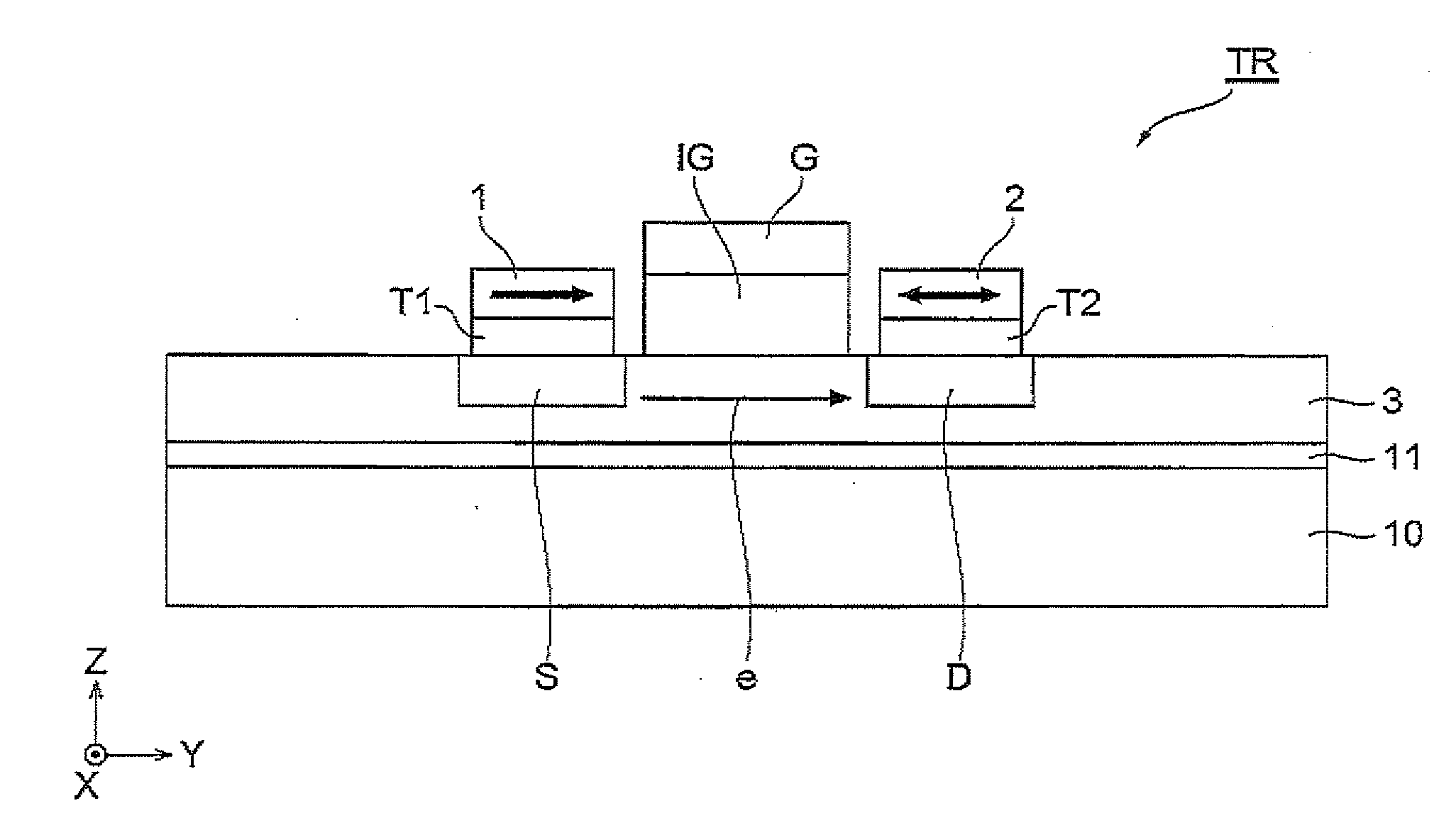
[0033]Hereinafter, a spin device according to an embodiment will be described. The same reference numerals are given to the same elements, and the duplicate explanation thereof will be omitted.
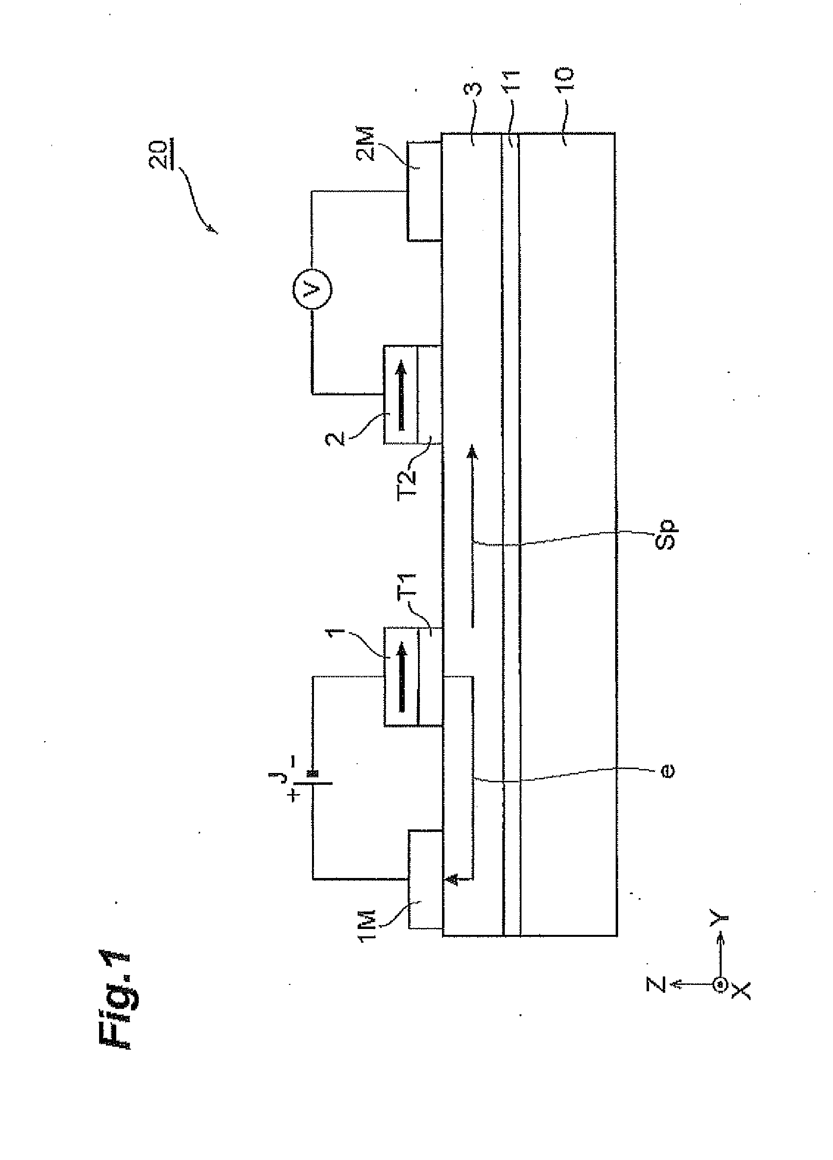
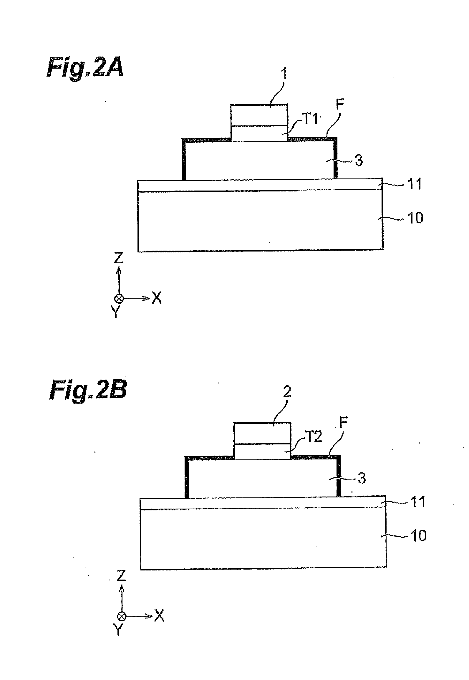
[0034]FIG. 1 is a diagram showing a longitudinal cross-sectional configuration of a spin device in a non-local structure. In FIG. 1, an XYZ three-dimensional Cartesian coordinate system is set. FIG. 2A is an XZ cross-sectional view in a position of a ferromagnetic metal layer 1 of the spin device shown in FIG. 1, and FIG. 2B is an XZ cross-sectional view in a position of a ferromagnetic metal layer 2 of the spin device.
[0035]A semiconductor layer 3 is formed on a semiconductor substrate 10 formed of Si via an insulating layer 11 of for example, SiO2 or Al2O3. That is, a substrate including the semiconductor layer 3 is an SOI (Silicon-on-Insulator) substrate, and a thickness of the semiconductor layer 3 is set to, for example, 100 inn or less. When the SOI substrate is used, the semiconductor l...
PUM
 Abstract
Description
Claims
Application Information