Memory Cell System and Method

a memory array and memory cell technology, applied in the field of memory cell systems and methods, can solve the problems of more susceptible to read disturbance, loss of data during read or write operations, behavior getting worse, etc., and achieve the effect of reducing the dynamic power consumed by the memory array

Inactive Publication Date: 2012-09-13
SHEPPARD DOUGLAS P
View PDF2 Cites 11 Cited by
  • Summary
  • Abstract
  • Description
  • Claims
  • Application Information

AI Technical Summary

Benefits of technology

[0066](9) Provide for a memory cell system and method that permits a reduction of dynamic power consumed by a memory array by utilizing a single Bit Line to access a given memory cell.

Problems solved by technology

This prior art methodology has the additional problem of having the ground power switch to the latch on the same side of the pass gate which makes it more susceptible to READ DISTURB.
Prior art approaches that adjust the power in the column direction incur a risk of disturbing all of the cells along the column and causing them to lose data during a read or write operation.
This behavior gets worse as transistor variations increase at smaller device geometries.
Instead, the prior art still relies on the pass gate to perform the read / write operation, leaving the memory cell susceptible to READ DISTURB.

Method used


Image

  • Memory Cell System and Method
  • Memory Cell System and Method
  • Memory Cell System and Method

Examples


embodiment

MULTI-WRITE Embodiment

Traditional Latch Write-1 Challenges (3500)

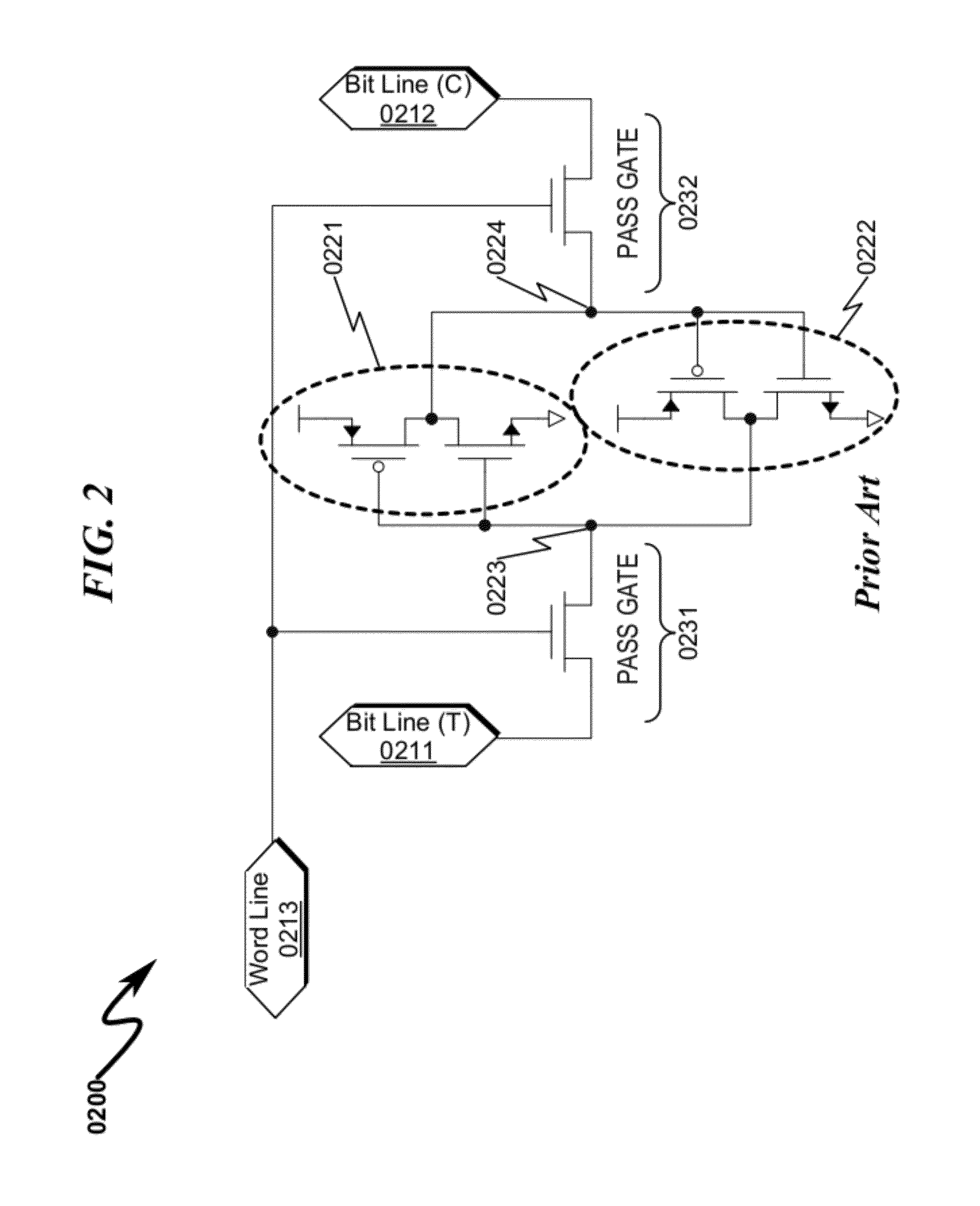
[0208]As mentioned in the Background Section, writing a “1” in the traditional 6T memory cell is difficult and requires a second Pass Gate to always have the ability to pull the high side low as shown in FIG. 35 (3500).

Cross-Coupled Latch Overview (3600)

[0209]A fundamental characteristic is the ability to easily write a high (“1) or low (“0”) into the cross coupled latch that makes up many different types of memory cells. A logic schematic of the cross coupled latch without the pass gates is illustrated in FIG. 36 (3600).

[0210]Reading and writing the memory cell latch has traditionally been achieved through additional circuitry that either passes the state of the latch out to be read or forces a high or a low onto the internal nodes of the latch (true (T), complement (C)) to the desired state of either a high or a low. An important embodiment is the ability to accomplish writing the more difficult state, such as a high...


PUM


Abstract

A memory cell system/method incorporating reduced transistor counts and/or improved design-for-manufacturability (DFM) is disclosed. The system/method incorporates cross-coupled feedthru (3410)/feedback (3420) amplifiers to implement memory cell state memory, wherein the feedback amplifier incorporates a multi-state output drive capability (3423) allowing the memory cell to be read/written using only one access device (3430) connected to the output (3412) of the feedthru (3410) amplifier. The multi-state output drive capability (3423) modulates the feedback amplifier (3420) drive strength to enable reading/writing of the feedthru amplifier (3410) state with greatly reduced memory cell input fan-in requirements. The invention anticipates replacement of traditional DP/8T/6T/4T memory cell structures with corresponding 6T/6T/5T/3T memory cell configurations, resulting in a 16%-25% transistor reduction depending on memory array application context.

Description

CROSS REFERENCE TO RELATED APPLICATIONS[0001]Applicant claims benefit pursuant to 35 U.S.C. §119 and hereby incorporates by reference Provisional patent application for “IMPROVED MEMORY CELL”, Ser. No. 61 / 451,031, docket ASHEP.0102P, filed electronically with the USPTO on Mar. 9, 2011.[0002]Applicant claims benefit pursuant to 35 U.S.C. §119 and hereby incorporates by reference Provisional patent application for “MEMORY CELL”, Ser. No. 61 / 452,845, docket ASHEP.0103P, filed electronically with the USPTO on Mar. 15, 2011.[0003]Applicant claims benefit pursuant to 35 U.S.C. §119 and hereby incorporates by reference Provisional patent application for “5T SINGLE PORT SRAM UTILIZING EASY-WRITE WITH IMPROVED NOISE MARGIN”, Ser. No. 61 / 476,098, docket ASHEP.0104P, filed electronically with the USPTO on Apr. 15, 2011.[0004]Applicant claims benefit pursuant to 35 U.S.C. §119 and hereby incorporates by reference Provisional patent application for “METHOD FOR WRITING AND READING A MEMORY WITH E...

Claims


Application Information

Patent Timeline
Patent Type & Authority Applications(United States)
IPC IPC(8): G11C7/00
CPCG11C8/14G11C11/412G11C11/418G11C7/08G11C7/06G11C7/00G11C7/10
Inventor SHEPPARD, DOUGLAS P.
Owner SHEPPARD DOUGLAS P
Why Eureka
Try Eureka