Image sensor with double integration time and conditional selection
a technology of image sensor and integration time, applied in the field of image sensor, can solve problems such as loss of dynamic range and interval reduction
- Summary
- Abstract
- Description
- Claims
- Application Information
AI Technical Summary
Benefits of technology
Problems solved by technology
Method used
Image
Examples
Embodiment Construction
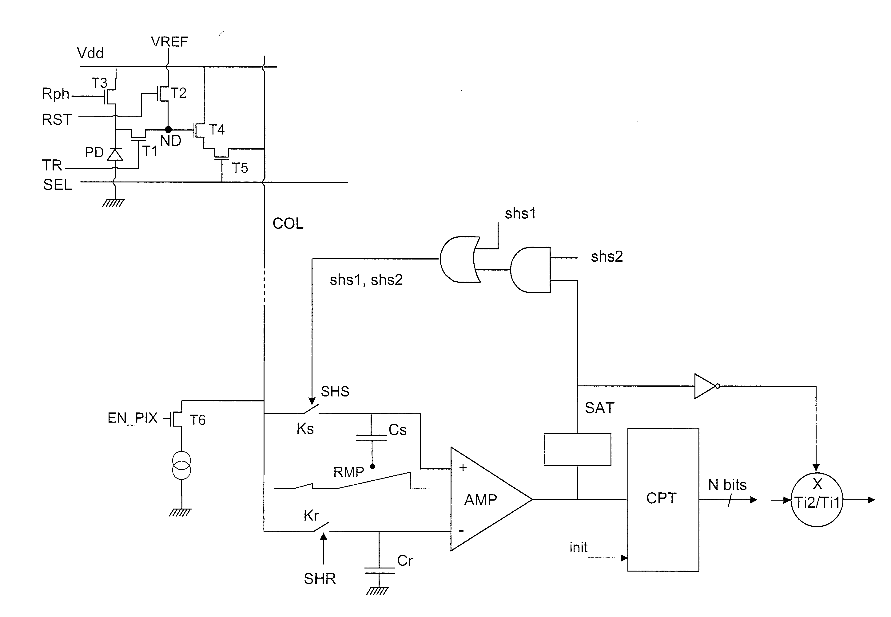
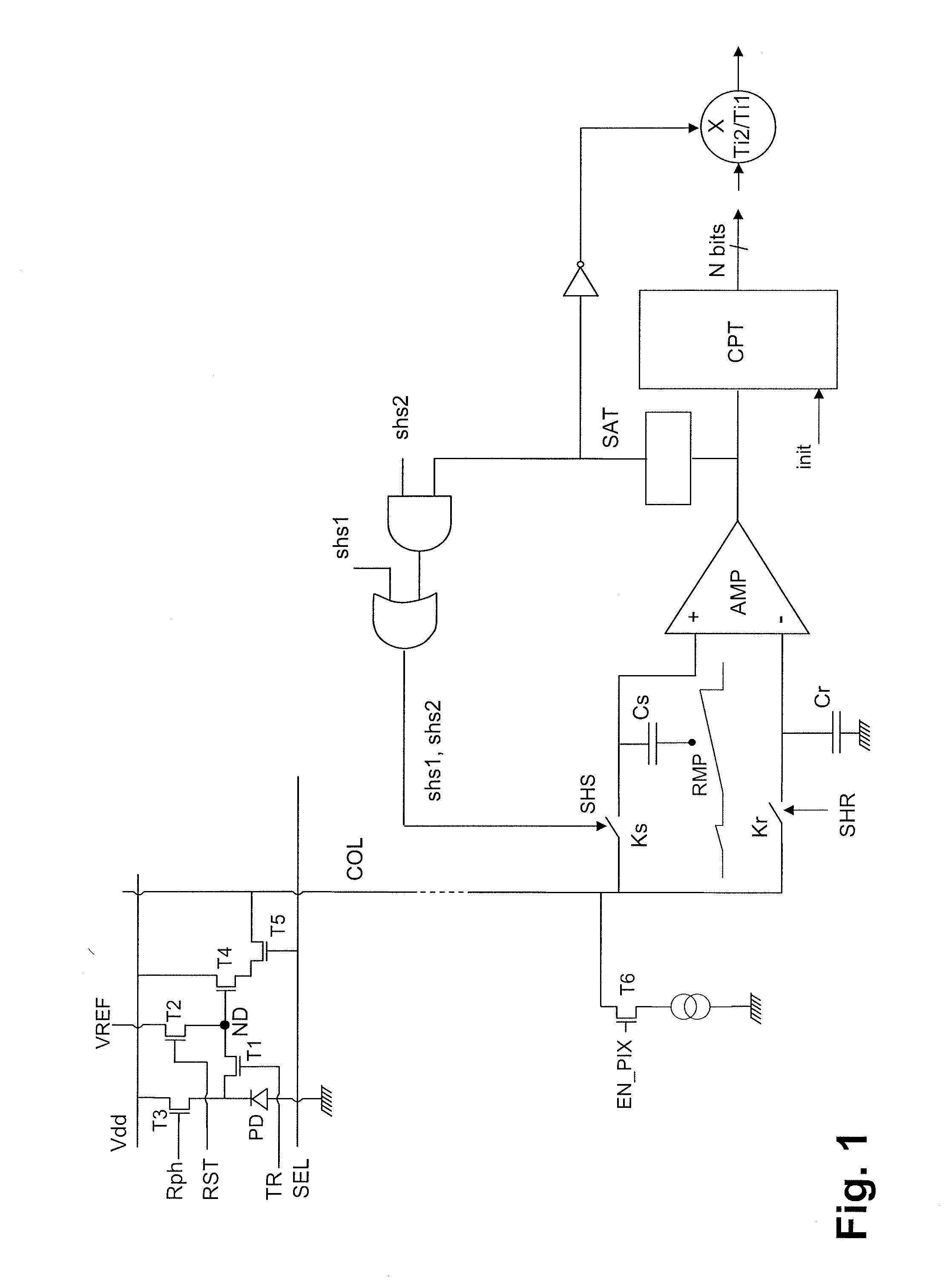
[0024]An active pixel with five transistors and a reading circuit of a sensor according to the invention are represented in FIG. 1. The structure of the pixel is conventional. It comprises a photodiode PD, a capacitive storage node ND (represented by a simple point in FIG. 1, and embodied in practice by an N-type diffusion in a P-type layer), a transistor for charge transfer T1 between the cathode of the photodiode and the storage node, a transistor T2 for reinitializing the potential of the storage node, a transistor T3 for reinitializing the potential of the photodiode, a follower transistor T4, a row selection transistor T5. For a pixel with four transistors the transistor T3 would be dispensed with.
[0025]The transfer transistor T1 is controlled by a transfer signal TR. The transistor T2 has its drain linked to a reference potential VREF and it is controlled by a reinitialization control signal RST. The transistor T3 is linked between the cathode of the photodiode and a reference...
PUM
 Abstract
Description
Claims
Application Information


