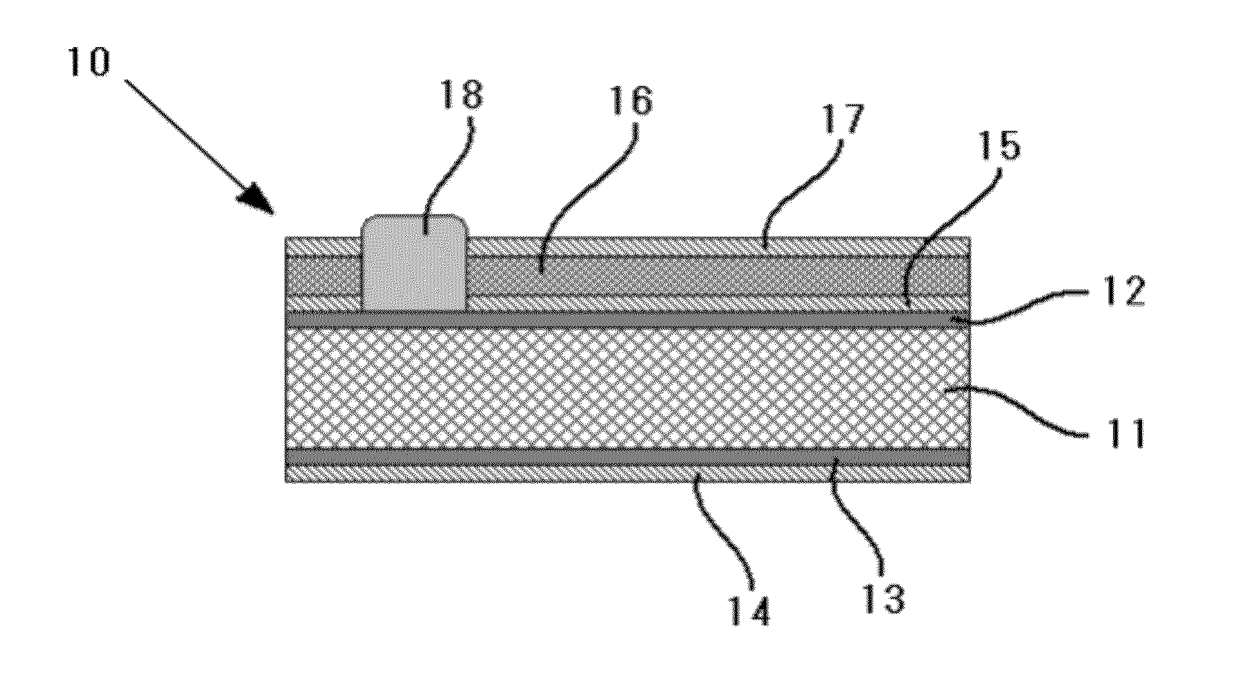
Metal nanowires, method for producing same, transparent conductor and touch panel
a technology of metal nanowires and transparent conductors, applied in the direction of conductors, conductive layers on insulating supports, instruments, etc., can solve the problems of unstable, high production cost, and high ratio of atoms exposed to surface (high energy and unstable), and achieve excellent heat resistance, excellent light transmission, and high electrical conductivity
- Summary
- Abstract
- Description
- Claims
- Application Information
AI Technical Summary
Benefits of technology
Problems solved by technology
Method used
Image

Examples
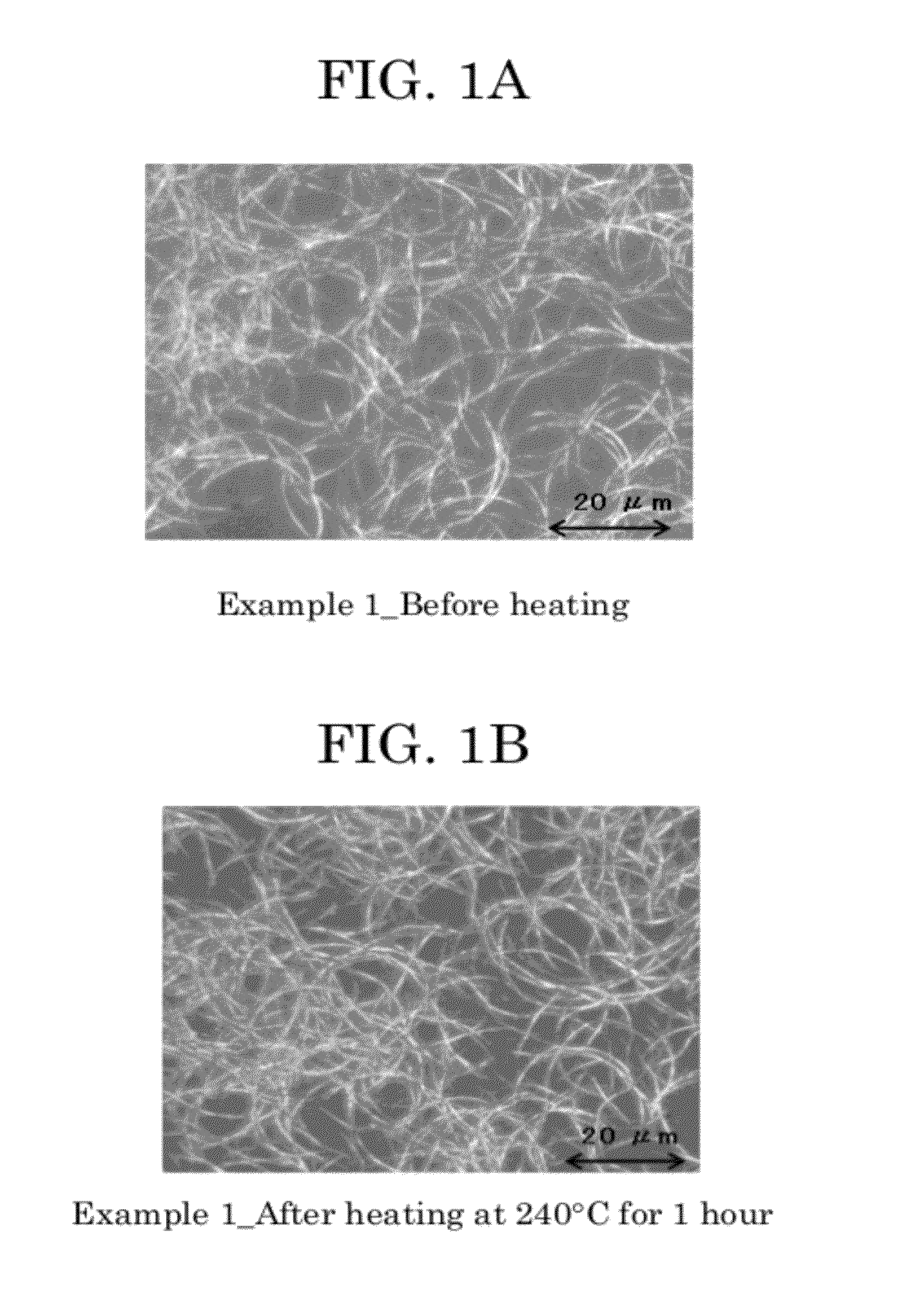
example 1
[0130]—Preparation of Additive Solution A—
[0131]In 50 mL of purified water, 0.51 g of silver nitrate powder was dissolved. Thereafter, 1N ammonia water was added until the solution became colorless and transparent. Then purified water was added such that the total amount became 100 mL to prepare an additive solution A. A desired amount of additive solution A was prepared by the preparation method.
[0132]—Preparation of Additive Solution B—
[0133]0.041 g of chloroauric acid tetrahydrate was dissolved in 100 mL of purified water to prepare 1 mM gold solution as an additive solution B. A desired amount of additive solution B was prepared by the preparation method.
[0134]—Preparation of Additive Solution C—
[0135]0.5 g of glucose powder was dissolved in 140 mL of purified water to prepare an additive solution C. A desired amount of additive solution C was prepared by the preparation method.
[0136]—Preparation of Additive Solution D—
[0137]0.5 g of HTAB (hexadecyltrimethylammonium bromide) pow...
example 2
[0148]The same process as in Example 1 was carried out except that the amount of chloroauric acid tetrahydrate, which is dissolved in 100 mL of purified water, in the preparation of additive solution B was changed from 0.041 g to 0.41 g, and metal nanowires of Example 2 containing 1.0 atomic % of gold were produced.
[0149]The metal nanowires of Example 2 were observed with a TEM. The average minor axis length and average major axis length of 200 particles were calculated and found to be 32.2 nm and 31.3 respectively.
[0150]The metal nanowires had a product of the amount of gold, P (atomic %), and the square root of the average minor axis length, φ (nm), i.e., P×φ0.5 of 5.7.
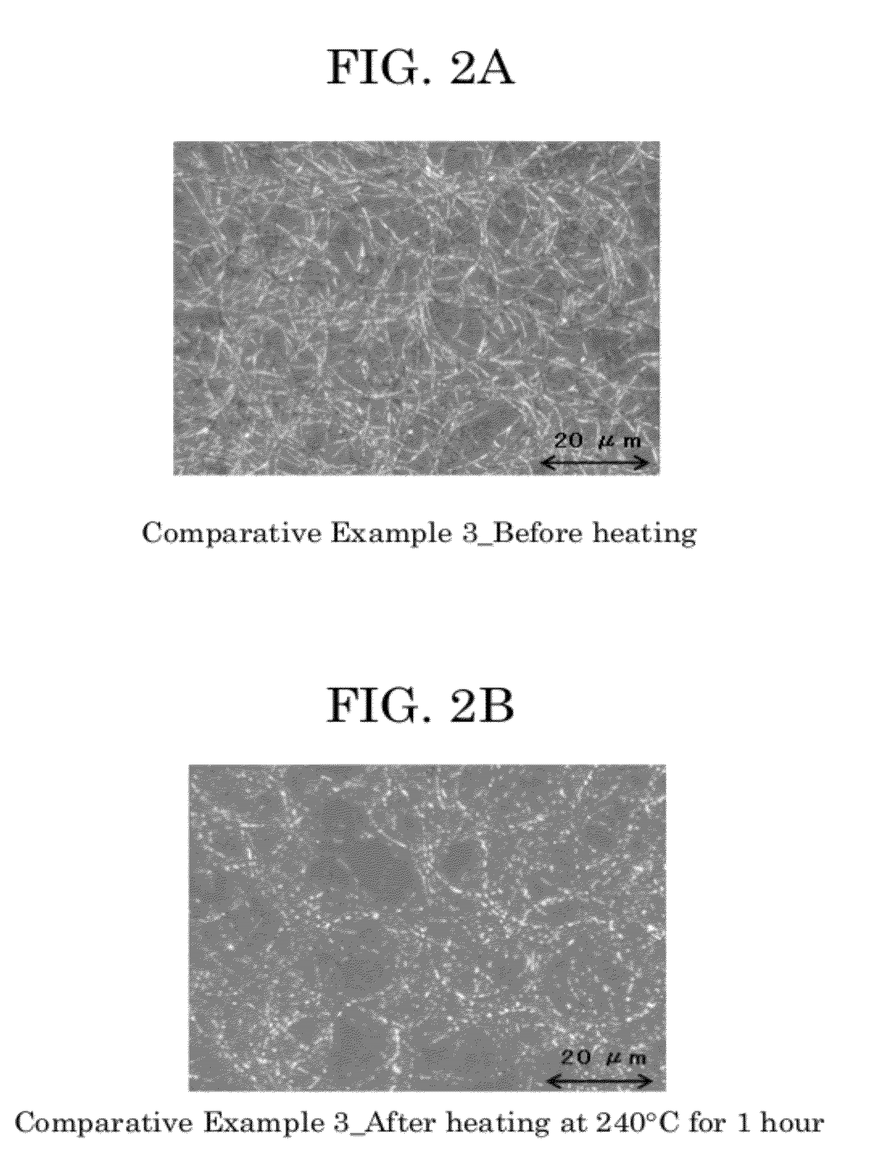
example 3
[0151]The same process as in Example 1 was carried out except that the amount of chloroauric acid tetrahydrate, which is dissolved in 100 mL of purified water, in the preparation of additive solution B was changed from 0.041 g to 0.0205 g, and metal nanowires of Example 3 containing 0.05 atomic % of gold were produced.
[0152]The metal nanowires of Example 3 were observed with a TEM. The average minor axis length and average major axis length of 200 particles were calculated and found to be 32.1 nm and 25.5 respectively.
[0153]The metal nanowires had a product of the amount of gold, P (atomic %), and the average minor axis length, φ (nm), i.e., P×φ of 0.28.
PUM
| Property | Measurement | Unit |
|---|---|---|
| length | aaaaa | aaaaa |
| length | aaaaa | aaaaa |
| transparent | aaaaa | aaaaa |
Abstract
Description
Claims
Application Information
 - R&D
- Intellectual Property
- Life Sciences
- Materials
- Tech Scout
- Unparalleled Data Quality
- Higher Quality Content
- 60% Fewer Hallucinations
Browse by: Latest US Patents, China's latest patents, Technical Efficacy Thesaurus, Application Domain, Technology Topic, Popular Technical Reports.
© 2025 PatSnap. All rights reserved.Legal|Privacy policy|Modern Slavery Act Transparency Statement|Sitemap|About US| Contact US: help@patsnap.com