Method of manufacturing organic electroluminescence device and method of setting laser focal position

a laser beam and laser beam technology, applied in the direction of organic semiconductor devices, semiconductor devices, electrical devices, etc., can solve the problems of difficult laser focus on the layer to be irradiated, inability to suppress damage on the peripheral portion, and difficult to solve, so as to solve the short circuit reliably and efficiently, solve the short circuit, and accurately determine the focal position of the laser beam

Active Publication Date: 2012-10-18
JOLED INC
View PDF1 Cites 9 Cited by
  • Summary
  • Abstract
  • Description
  • Claims
  • Application Information

AI Technical Summary

Benefits of technology

[0013]An object of the present invention, in view of the problem above, is to provide a method of manufacturing an organic EL device and a method of setting a laser focal position that allow setting a laser focus on a specific layer in a multilayer organic EL device so as to solve a shorted portion reliably and efficiently.
[0014]To solve the problem described above, a method of manufacturing an organic electroluminescence (EL) device according to an aspect of the present invention includes: preparing an organic EL device in which a lower electrode layer, an organic layer including a luminescent layer, and an upper electrode layer are stacked in order and in which at least one of the lower electrode layer and the upper electrode layer is formed of a transparent material, the organic EL device including a defective portion; irradiating the organic EL device including the defective portion with a laser beam from a direction of the at least one of the upper and lower electrode layers that is formed of the transparent material; measuring an intensity of radiated light that is light radiated from the organic EL device after the laser beam is absorbed through multiphoton absorption; determining a focal position of the laser beam in a stacking direction such that the intensity of the radiated light is minimal, after changing the focal position of the laser beam in the stacking direction for performing the irradiating and the measuring; and emitting the laser beam onto the organic EL device at the determined focal position in the stacking direction so as to solve a defect caused by the defective portion.
[0015]With the method of manufacturing an organic electroluminescence device according to the present invention, it is possible to determine the focal position of the laser beam accurately using the intensity of radiated light that is light radiated through multiphoton absorption or the intensity of radiated light detected at a side of a wavelength shorter than a wavelength of the emitted laser beam, thus reliably solving the short circuit between the anode and the cathode while suppressing occurrence of a damage caused by laser irradiation. This accordingly realizes highly efficient repair and increases manufacturing yield.

Problems solved by technology

However, in the case of applying the laser focus control method disclosed in Patent Reference 5 to a multilayer such as the organic EL device, multiple reflection light is obtained from each layer interface, which does not allow extracting and monitoring only the laser light reflected from a layer that is an irradiation target point, thus making it difficult to focus the laser on the layer to be irradiated.
Accordingly, in the case of using the method of controlling the laser focus as described above, it is difficult to solve the short-circuit state of the organic EL device, so that it is not possible to suppress the damage on a peripheral portion thereof even if the short-circuit state can be solved.
Thus, the organic EL device after laser repair cannot ensure performance such as luminance efficiency and product cycle, thus making it difficult to improve repair efficiency and increase manufacturing yield.

Method used


Image

  • Method of manufacturing organic electroluminescence device and method of setting laser focal position
  • Method of manufacturing organic electroluminescence device and method of setting laser focal position
  • Method of manufacturing organic electroluminescence device and method of setting laser focal position

Examples


first embodiment

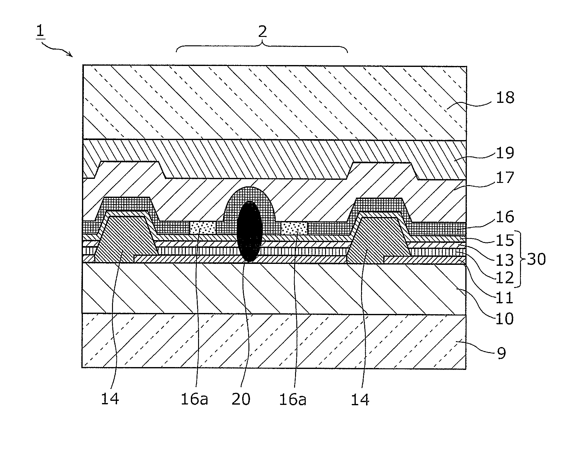
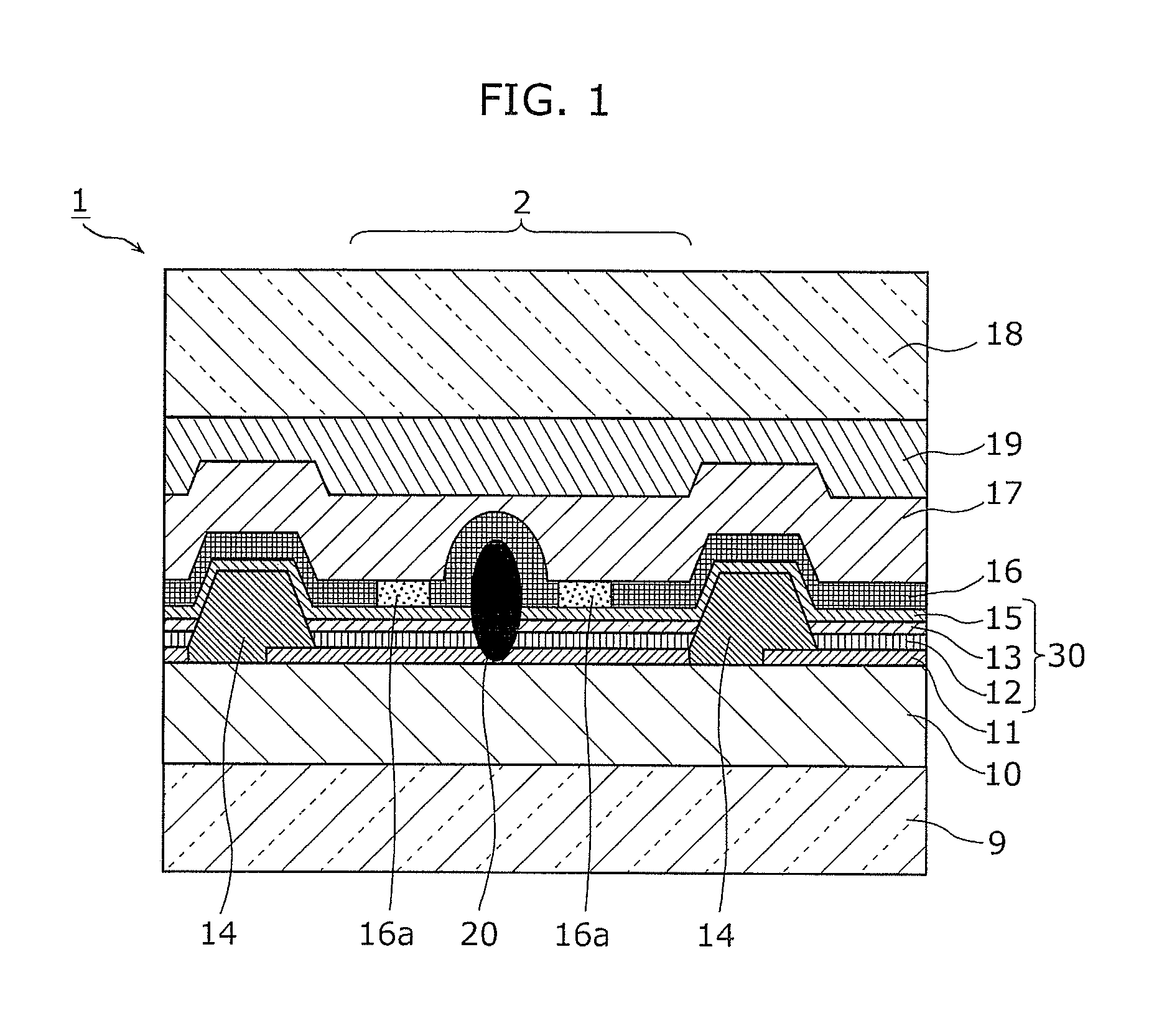
[0056]FIG. 1 is a schematic cross-sectional view of an organic EL device according to a first embodiment of the present invention. An organic EL device 1 shown in the figure is an organic functional device including an anode, a cathode, and an organic layer interposed between the two electrodes and including a luminescent layer.

[0057]As shown in FIG. 1, the organic EL device 1 includes, on a transparent glass 9, a flattening film 10, an anode 11, a hole injection layer 12, a luminescent layer 13, a bank 14, an electron injection layer 15, a cathode 16, a thin-film encapsulating layer 17, an encapsulating resin layer 19, and a transparent glass 18.

[0058]The anode 11 and the cathode 16 correspond, respectively, to a lower electrode layer and an upper electrode layer according to the present invention. In addition, the hole injection layer 12, the luminescent layer 13, and the electron injection layer 15 correspond to the organic layer in the present invention.

[0059]The transparent gla...


PUM


Abstract

A method of manufacturing an organic electroluminescence device includes: preparing an organic EL device in which an anode, an organic layer including a luminescent layer, and a cathode formed of a transparent material are stacked in order and which has a shorted defective portion; irradiating the organic EL device with a laser beam from a direction of the cathode; measuring an intensity of radiated light from the organic EL device after the laser beam is absorbed through multiphoton absorption; changing a focal position of the laser beam in a stacking direction for performing the irradiating and measuring, and subsequently determining the focal position of the laser beam in the stacking direction such that the intensity of the radiated light is minimal; and irradiating the determined focal position with the laser beam, so as to solve a defect caused by the shorted defective portion.

Description

CROSS REFERENCE TO RELATED APPLICATION[0001]This is a continuation application of PCT Patent Application No. PCT / JP2011 / 002149 filed on Apr. 12, 2011, designating the United States of America. The entire disclosure of the above-identified application, including the specification, drawings, and claims are incorporated herein by reference in its entirety.BACKGROUND OF THE INVENTION[0002](1) Field of the Invention[0003]The present invention relates to a method of manufacturing an organic electroluminescence device and a method of setting a laser focal position.[0004](2) Description of the Related Art[0005]Conventionally, in an organic electroluminescence (hereinafter, referred to as an organic EL) device including an organic layer interposed between an anode and a cathode, there is a case where a short circuit is caused between the anode and the cathode due to attachment or mixture of a conductive foreign substance during the manufacturing process. In this case, there is a method of re...

Claims


Application Information

Patent Timeline
Patent Type & Authority Applications(United States)
IPC IPC(8): H01L51/56
CPCH01L2251/568H01L51/56H10K71/861H10K71/00H10K50/11H10K50/00
Inventor HIRAOKA, TOMOMISEGAWA, YASUO
Owner JOLED INC
Why Eureka
Try Eureka