Solid-state imaging device and method for manufacturing the same

a solid-state imaging and imaging device technology, applied in semiconductor/solid-state device manufacturing, semiconductor devices, electrical devices, etc., can solve the problems of void formation, inability to fully increase the refractive index, and the light collecting performance of the optical waveguide cannot fully increase, so as to achieve high light collecting performance, easy implementation, and high refractive index

Inactive Publication Date: 2012-10-25
PANASONIC CORP
View PDF16 Cites 10 Cited by
  • Summary
  • Abstract
  • Description
  • Claims
  • Application Information

AI Technical Summary

Benefits of technology

[0032]With the solid-state imaging device and method for manufacturing the same of the present invention, a solid-state imaging device including

Problems solved by technology

When deposition is carried out into a concave portion whose aspect ratio is high using a vapor-state raw material, voids may be formed because of insufficient supply of the raw material into the concave portion.
However, in the case where the concave portion is filled with the resin, it is associated with a problem that the light collect

Method used


Image

  • Solid-state imaging device and method for manufacturing the same
  • Solid-state imaging device and method for manufacturing the same
  • Solid-state imaging device and method for manufacturing the same

Examples


Embodiment Construction

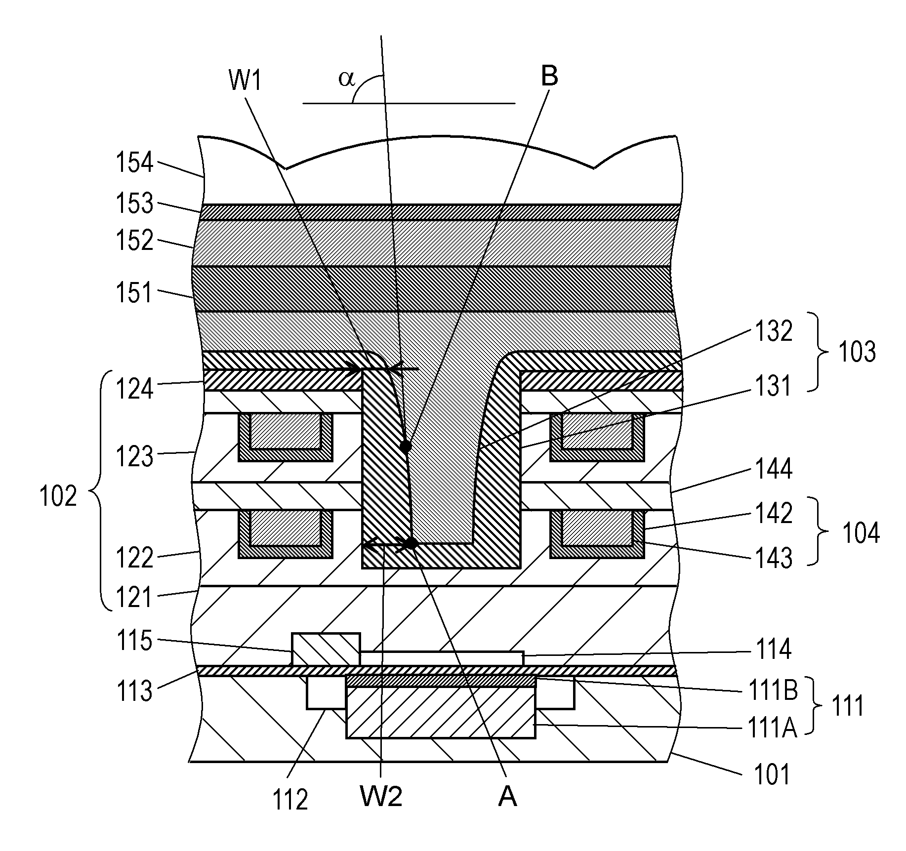
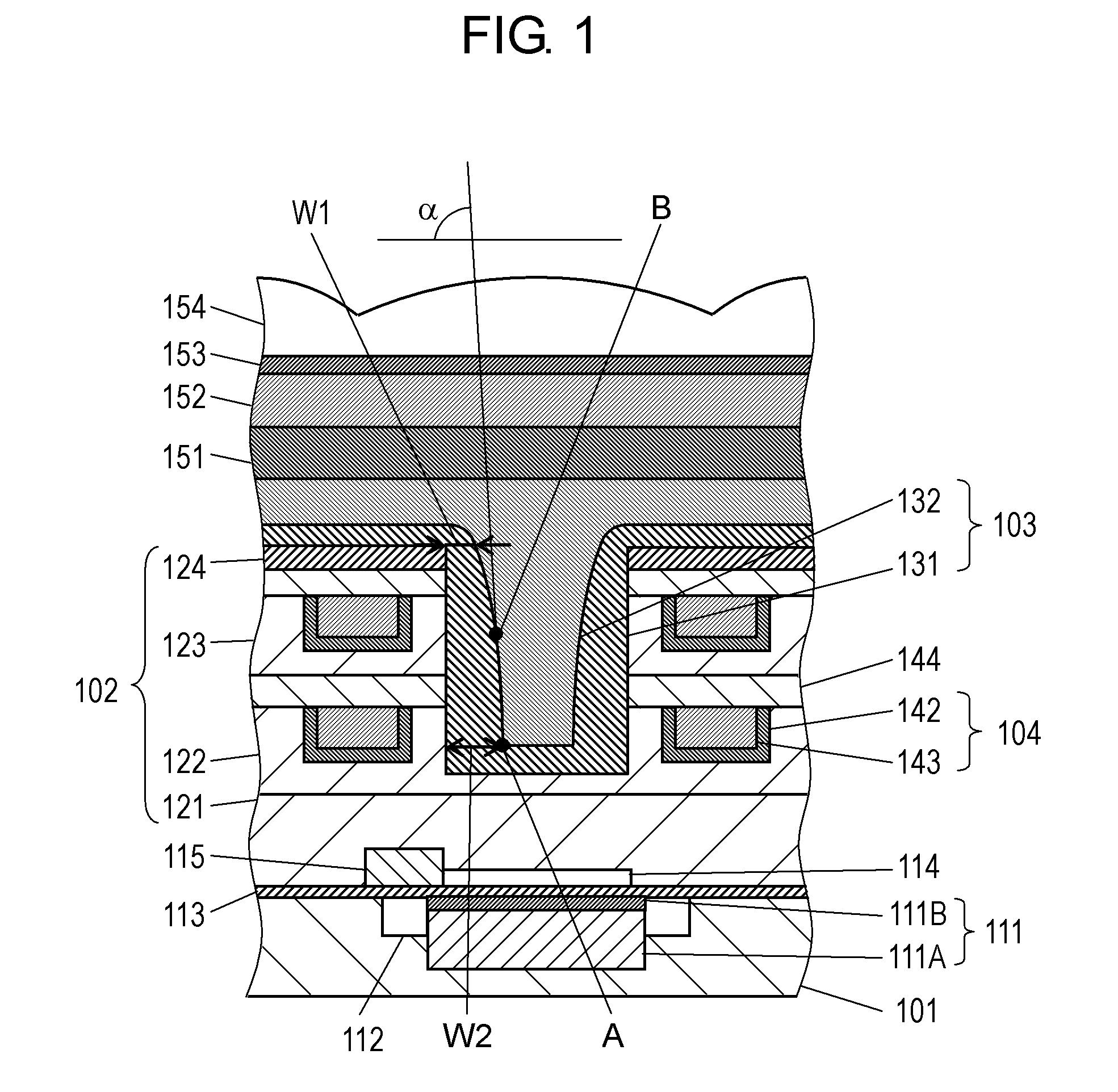
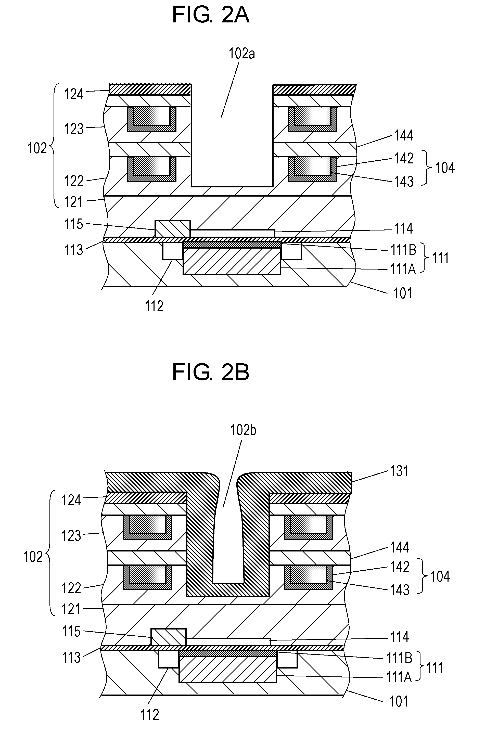
[0050]FIG. 1 shows one pixel in a solid-state imaging device according to one embodiment. As shown in FIG. 1, the solid-state imaging device of the present embodiment is a Complementary Metal Oxide Semiconductor (CMOS) sensor. A pixel including light receiving element 111 is formed on a light receiving face of substrate 101 of a silicon substrate or the like. On substrate 101, multilayer structure 102 and optical waveguide 103 embedded in multilayer structure 102 are formed.

[0051]Light receiving element 111 may be a photodiode in which a pn junction is formed by n type charge storage layer 111A and p+ type surface layer 111B. Beside light receiving element 111 in substrate 101, element isolation region 112 is formed. Element isolation region 112 may be formed by injecting impurities such as boron through ion injection into a prescribed region of substrate 101. On substrate 101, gate insulating film 113 made of silicon oxide (SiO2) or the like is formed.

[0052]On gate insulating film ...


PUM


Abstract

A solid-state imaging device includes: a light receiving portion formed on a semiconductor substrate; a multilayer structure formed on the semiconductor substrate, that includes an interlayer insulating film and a first concave portion at a position corresponding to the light receiving portion; and an optical waveguide formed in the first concave portion. The optical waveguide includes a first film and a second film formed sequentially from a side of the multilayer structure. The first film covers a side face and a bottom face of the first concave portion and includes a second concave portion. The second film is in contact with the first film and fills up the second concave portion. The thickness of the first film formed on the side face of the first concave portion is thinner at a top portion of the first concave portion than at the bottom portion thereof.

Description

BACKGROUND[0001]1. Technical Field[0002]The present invention relates to a solid-state imaging device and a method for manufacturing the same, and in particular, to a solid-state imaging device including an optical waveguide and a method for manufacturing the same.[0003]2. Description of the Related Art[0004]In recent years, while pixels are miniaturized and densely packed as solid-state imaging devices are reduced in size and hence the light receiving region is reduced, there are demands for higher sensitivity. In order to achieve compatibility between a reduction in the light receiving region and higher sensitivity, various structures for allowing light to enter a light receiving element more efficiently are considered. For example, there is a structure in which an on-chip lens is provided on a color filter so that light is efficiently collected for a light receiving element. Another structure is provided with an optical waveguide on a light receiving element, so that incident lig...

Claims


Application Information

Patent Timeline
IPC IPC(8): H01L31/0232H01L31/18
CPCH01L27/14685H01L27/14629
Inventor SUZUKI, SHIGERUOHNAKA, HIROFUMIYAMAMOTO, KOUICHI
Owner PANASONIC CORP
Why Eureka
Try Eureka