

Method for manufacturing a solar cell
- Summary
- Abstract
- Description
- Claims
- Application Information
AI Technical Summary
Benefits of technology
Problems solved by technology
Method used
Image

Examples
Embodiment Construction
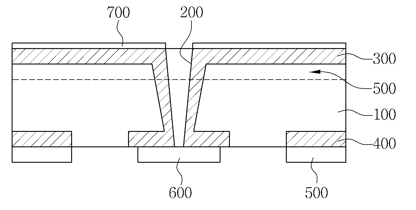
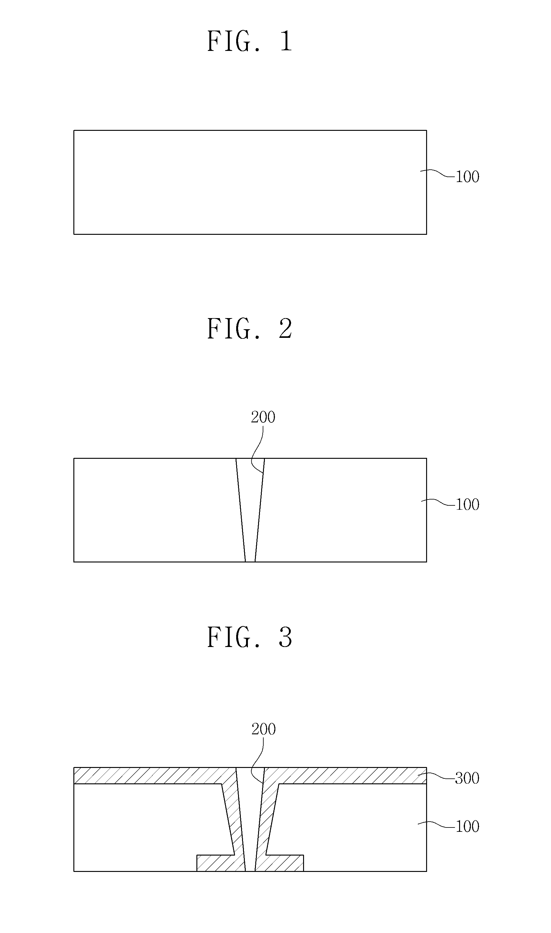
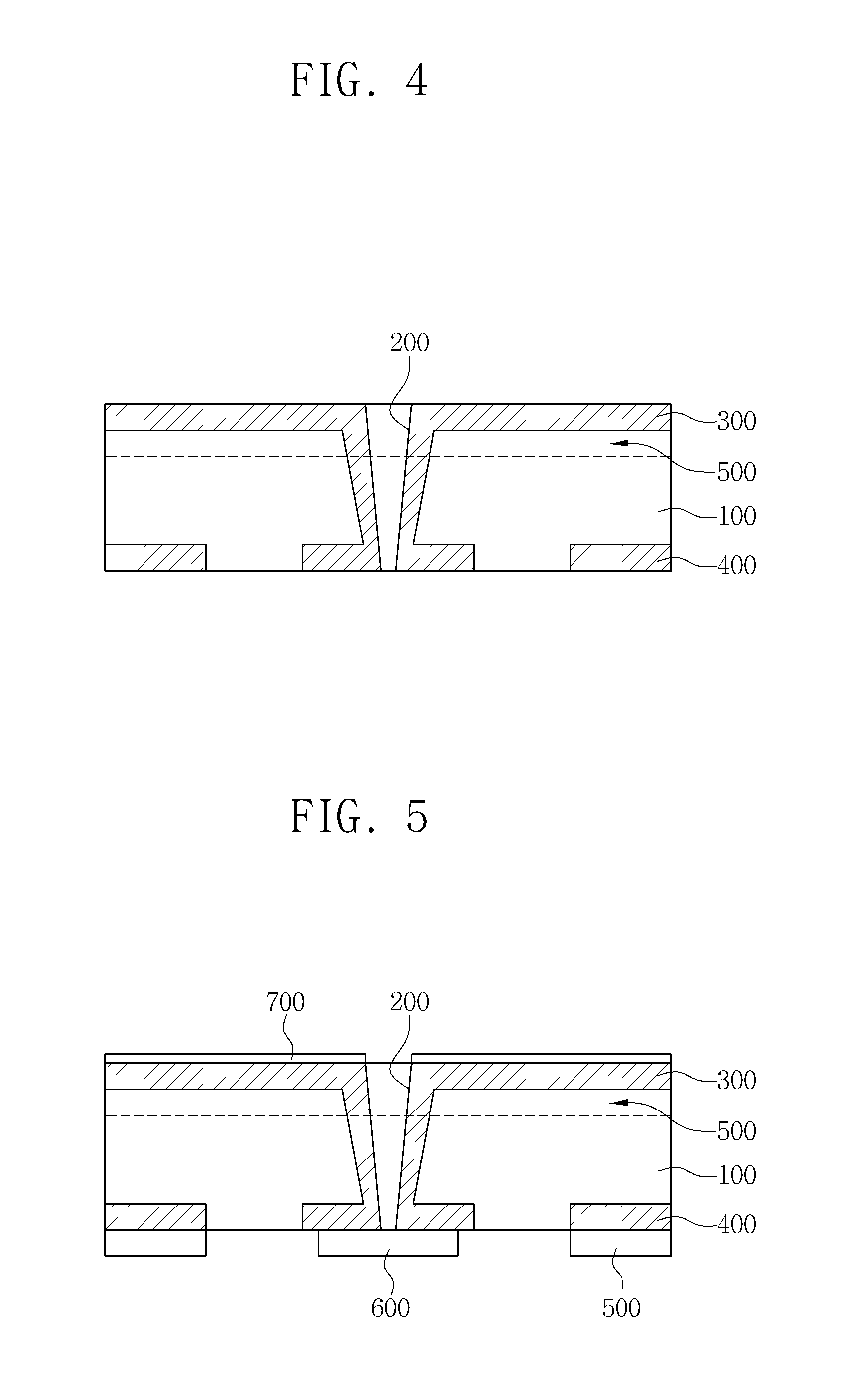
[0040]Meanwhile, referring to FIG. 6, the shallow emitter 300 is formed first, and after the selective emitter 500 is formed by heavy doping, the PSG left due to diffusion is removed. Then, the silicon nitride layer is deposited on the front and rear surfaces of the wafer 100 using chemical vapor deposition (CVD) and Al is printed on the rear surface of the wafer 100.
[0041]Then, Ag is printed on the rear surface of the wafer 100. In this case, the fine line finger 700 is formed so as to be connected to the via holes 200 along a direction of linking the via holes 200.
[0042]Plating is performed during a metal forming process to perform a solar cell test process.
[0043]Referring to FIGS. 7 and 8, the height H2, width W2, and the cross-sectional area of the fine line finger 700 are 9 μm, 60 μm, and 270 μm2 respectively.
[0044]When compared to the general fine line finger 700 of FIG. 7 with the assumption that the height H1, width W1, and the cross-sectional area of the general fine line f...
PUM
 Abstract
Description
Claims
Application Information