Method for manufacturing single crystal silicon solar cell and single crystal silicon solar cell

Inactive Publication Date: 2009-01-08
SHIN ETSU CHEM CO LTD
21 Cites 27 Cited by

AI-Extracted Technical Summary

Problems solved by technology

In addition, amorphous silicon solar cells still suffer from deterioration of the output characteristics under light irradiation.
However, even with such a method employing zone melt...

Benefits of technology

[0037]In this manner, when an interior of the transparent insulator substrate or a surface thereof opposite to a surface near the single crystal silicon layer is capable of scattering light; the surface of the transparent insulator substrate near the single crystal silicon layer is capable of scattering light; or the transparent adhesive layer is capable of scattering light; the optical path length of the light incident on the single crystal silicon layer serving as a light-converting layer can further be extended, resulting in a thin-film single crystal silicon solar cell with an optical-confinement structure, in which more light can be absorbed by the single crystal sil...

Abstract

A method for manufacturing a single crystal silicon solar cell includes the steps of implanting either hydrogen ions or rare-gas ions into a single crystal silicon substrate; bringing the single crystal silicon substrate in close contact with a transparent insulator substrate via a transparent adhesive, with the ion-implanted surface being a bonding surface; curing the transparent adhesive; mechanically delaminating the single crystal silicon substrate to form a single crystal silicon layer; forming a plurality of diffusion areas of a second conductivity type in the delaminated surface side of the single crystal silicon layer, and causing a plurality of areas of a first conductivity type and the plurality of areas of the second conductivity type to be present in the delaminated surface of the single crystal silicon layer; forming each of a plurality of individual electrodes on each one of the plurality of areas of the first conductivity type and on each one of the plurality of areas of the second conductivity type in the single crystal silicon layer; forming a collector electrode for the plurality of individual electrodes on the plurality of areas of the first conductivity type, and a collector electrode for the plurality of individual electrodes on the plurality of areas of the second conductivity type; and forming a light-reflecting film.

Application Domain

Final product manufactureSemiconductor/solid-state device manufacturing +4

Technology Topic

Monocrystalline siliconAdhesive +8

Image

  • Method for manufacturing single crystal silicon solar cell and single crystal silicon solar cell
  • Method for manufacturing single crystal silicon solar cell and single crystal silicon solar cell
  • Method for manufacturing single crystal silicon solar cell and single crystal silicon solar cell

Examples

  • Experimental program(4)

Example

Example 1
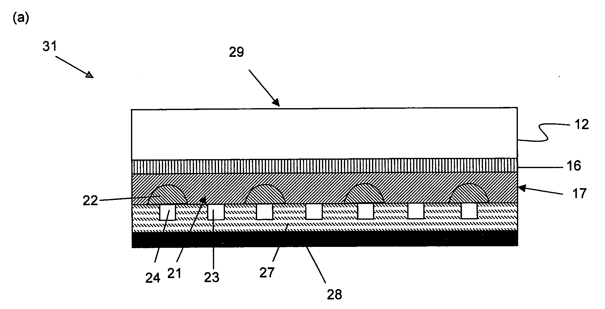
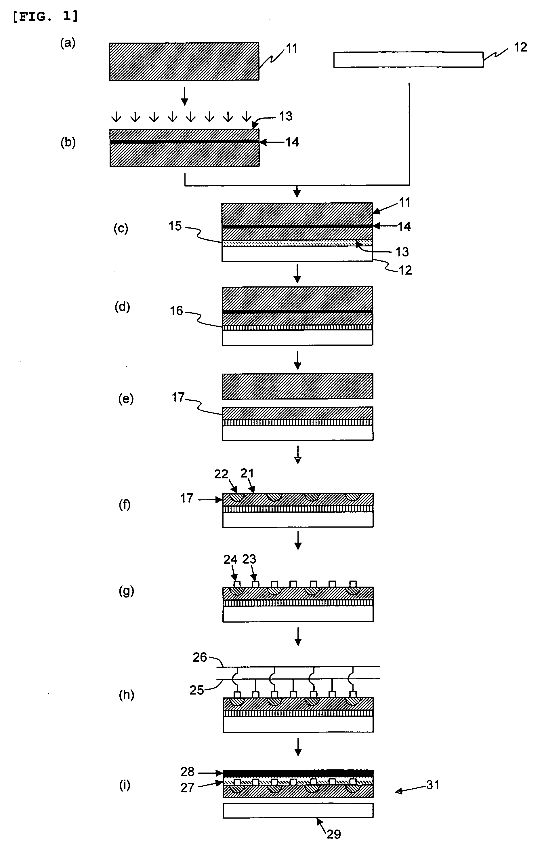
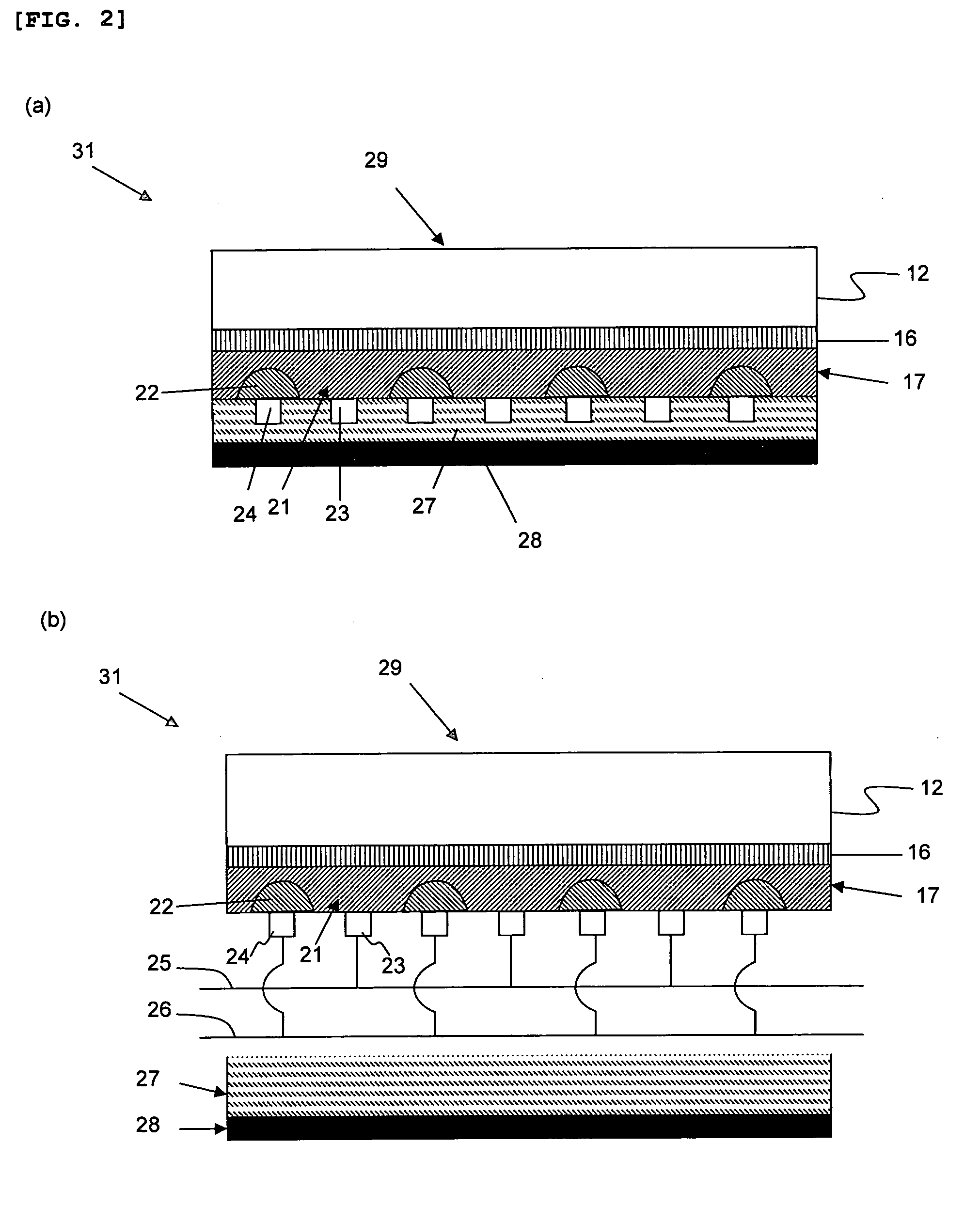
[0098]A single crystal silicon substrate with a diameter of 200 mm (8 inches), the crystal plane (100), the p-type conductivity, and a surface resistance of 15 Ωcm was prepared as a single crystal silicon substrate 11. A quartz glass substrate with a diameter of 200 mm (8 inches) and a thickness of 2.5 mm was also prepared as a transparent insulator substrate 12 (Step a).
[0099]H+ ions were then implanted into one main surface of the single crystal silicon substrate 11 at a dose of 1.0×10¹⁷/cm2 and at an energy level of 350 keV (Step b). An ion-implanted layer 14 was thus formed at a depth of about 3 μm from the ion-implanted surface 13.
[0100]A polycondensate was obtained by hydrolysis and polycondensation of an alkyltrialkoxysilane and a tetraalkoxysilane using hydrochloric acid as a catalyst. The product was dissolved in isopropyl alcohol solvent to give a transparent adhesive (silicone resin). The single crystal silicon 11 and the quartz glass substrate 12 were brought in close contact via the transparent adhesive 15 (Step c).
[0101]The bonded substrate was heat-treated at 250° C. for two hours, and then returned to room temperature, thereby curing the transparent adhesive 15 to form a transparent adhesive layer 16. Simultaneously, the single crystal silicon 11 and the quartz glass substrate 12 were firmly bonded (Step d).
[0102]A high-pressure nitrogen gas was then applied near the ion-implanted layer at room temperature, and then the single crystal silicon substrate was mechanically delaminated so that delamination started from the nitrogen gas-applied surface (Step e). The delamination was performed after adhering an auxiliary substrate to the rear surface of each of the single crystal silicon substrate and the quartz glass substrate. The single crystal silicon layer 17 obtained through delamination and transfer was subsequently heat-treated by a flash-lamp annealing method so that the surface thereof was instantaneously heated to 700° C. or higher, to recover the damage due to hydrogen implantation.
[0103]Using a diffusion paste containing phosphorus glass and ethylcellosolve as a thickner, a pattern with a line width of 50 μm was formed on the surface of the single crystal silicon layer 17 at an interval of 1 mm by a screen printing method. The pattern was subjected to flash-lamp radiation so that the surface thereof was instantaneously heated to 600° C. or higher, thereby forming a plurality of n-type diffusion areas 22 at a junction depth of about 0.2 μm (Step f). This resulted in the p-type areas 21 and the n-type areas 22 being alternately present on the surface of the single crystal silicon layer 17, and a plurality of pn junctions being formed in the plane direction of the single crystal silicon layer.
[0104]After removing and cleaning the diffusion paste with fluoric acid and acetone or isopropyl alcohol, each of a plurality of first individual electrodes 23 was formed on each one of the plurality of p-type areas 21, and each of a plurality of second individual electrodes 24 was formed on each one of the plurality of n-type areas 22, using silver as an electrode material, by a vacuum evaporation method and a patterning method (Step g).
[0105]After this, using silver as an electrode material, a first collector electrode 25 was formed to connect the plurality of first individual electrodes 23, and a second collector electrode 26 was formed to connect the plurality of second individual electrodes 24, by a vacuum evaporation method employing a metal mask (Step h).
[0106]A silicon nitride coating as a seal layer 27 was then formed, using a reactive sputtering method, on the surface of the single crystal silicon layer 17 excluding the portion of the electrodes through which electricity is obtained. An alumite-treated aluminum film was then bonded as a light-reflecting film 28 onto the seal layer 27 via polyvinyl butyral as an adhesive (Step i).
[0107]In this manner, the thin-film single crystal silicon solar cell 31 shown in FIGS. 2 (a) and (b) was fabricated. The solar cell 31 comprises a stack having the aluminum light-reflecting film 28, silicon nitride seal layer 27, single crystal silicon layer 17, transparent adhesive layer 16, and quartz glass substrate 12. The plurality of p-type areas 21 and the plurality of n-type areas 22 are formed in the surface of the single crystal silicon layer 17 near the light-reflecting film 28, and the plurality of pn junctions are formed at least in the plane direction of the single crystal silicon layer. Each of the plurality of first individual electrodes 23 is formed on each one of the plurality of p-type areas 21, and each of the plurality of second individual electrodes 24 is formed on each one of the plurality of n-type areas 22 on the single crystal silicon layer 17. The first collector electrode 25 for connecting the plurality of first individual electrodes 23 and the second collector electrode 26 for connecting the plurality of second individual electrodes 24 are formed.
[0108]The single crystal silicon solar cell thus fabricated was irradiated with 100 mW/cm2 of light through the light-receiving surface 29 of the quartz glass substrate 12, using a solar simulator at AM 1.5, to measure the conversion efficiency. The conversion efficiency was 12.5% without any change over time.
[0109]Although the light-converting layer was as thin as 3 μm, the thin-film single crystal silicon solar cell exhibited a high conversion efficiency. Such a high conversion efficiency was considered to be obtained because the silicon layer serving as a light-converting layer was composed of single crystal silicon with satisfactory crystallinity, and the optical-confinement structure was employed.

Example

Example 2
[0110]A light-scattering layer was additionally formed on a light-receiving surface 29 of a quartz glass substrate 12 of a single crystal silicon solar cell as fabricated in Example 1, as follows. A polycondensate resin which was obtained by hydrolysis and polycondensation of an alkyltrialkoxysilane and a tetraalkoxysilane using hydrochloric acid as a catalyst, and which contained 60% by weight of zirconium oxide particles with an average particle size of 0.3 μm and a refractive index of 2.4, was dissolved in isopropyl alcohol solvent to form a transparent resin material. The transparent resin material was then applied onto the quartz glass substrate 12 to a thickness of 2 μm.
[0111]The single crystal silicon solar cell thus having a light-scattering capability on the light-receiving surface 29 of the quartz glass substrate 12 was measured for conversion efficiency in the same manner as in Example 1. As a result, the conversion efficiency was 15% without any change over time.
[0112]Owing to a further improvement in the optical-confinement structure, the conversion efficiency became higher than that of Example 1.

Example

Example 3
[0113]A thin-film single crystal silicon solar cell 31 was fabricated in the same manner as in Example 1, except that a quartz glass substrate 12 in which both surfaces have irregularities with a size of about 0.1 μm was used.
[0114]The single crystal silicon solar cell thus having a light-scattering capability on the interface of the quartz glass substrate 12 with the transparent adhesive layer 16 was measured for conversion efficiency in the same manner as in Example 1. As a result, the conversion efficiency was 16% without any change over time.
[0115]Owing to a further improvement in the optical-confinement structure, the conversion efficiency became higher than that of Example 1.

PUM

no PUM

Description & Claims & Application Information

We can also present the details of the Description, Claims and Application information to help users get a comprehensive understanding of the technical details of the patent, such as background art, summary of invention, brief description of drawings, description of embodiments, and other original content. On the other hand, users can also determine the specific scope of protection of the technology through the list of claims; as well as understand the changes in the life cycle of the technology with the presentation of the patent timeline. Login to view more.

Similar technology patents

Compound solar cell and process for producing the same

InactiveUS20050284518A1conversion efficiency be enhanceincrease voc
Owner:NAT INST OF ADVANCED IND SCI & TECH

Semiconductor device

InactiveUS20100001790A1reduce parasitic inductanceconversion efficiency be high
Owner:RENESAS ELECTRONICS CORP

Process for production of 1,2,2,2-tetrafluoroethyl difluoromethyl ether (desflurane)

InactiveUS20100185020A1conversion efficiency be highhigh yield and purity
Owner:PIRAMAL ENTERPRISES LTD

Solar light collecting method in multi-tower beam-down light collecting system

InactiveUS20110259320A1conversion efficiency be enhance
Owner:COSMO OIL CO LTD +1

Dye-sensitized solar cell and dye-sensitized solar cell module

InactiveUS20120042930A1high yieldconversion efficiency be high
Owner:SHARP KK

Photoelectric conversion device

ActiveUS20120211066A1conversion efficiency be high
Owner:SEMICON ENERGY LAB CO LTD

Architecture of power supply system for LCD apparatus

InactiveUS20050237010A1conversion efficiency be high
Owner:DELTA ELECTRONICS INC

Classification and recommendation of technical efficacy words

  • conversion efficiency be enhance

Compound solar cell and process for producing the same

InactiveUS20050284518A1conversion efficiency be enhanceincrease voc
Owner:NAT INST OF ADVANCED IND SCI & TECH

Solar light collecting method in multi-tower beam-down light collecting system

InactiveUS20110259320A1conversion efficiency be enhance
Owner:COSMO OIL CO LTD +1
Why Eureka
Try Eureka