
Compound solar cell and process for producing the same

Inactive Publication Date: 2005-12-29
NAT INST OF ADVANCED IND SCI & TECH
View PDF1 Cites 50 Cited by
  • Summary
  • Abstract
  • Description
  • Claims
  • Application Information

AI Technical Summary

Benefits of technology

[0018] An object of the present invention is to enhance conversion efficiency of a solar cell by realizing the ohmic contact without using an expensive metal, such as Pt, Pd or Ir, to thereby increase Voc to the utmost extent.

Problems solved by technology

Even though conversion efficiency realized in the CIGS solar cell is improved, it is considerably lower than the value theoretically expected.
Therefore, as the reason why the open circuit voltage is low, band mismatch in the contact between the light-absorbing layer and the back electrode is suspected.
However, it is difficult to optionally control the formation of MoSe2 and MoSe2 itself is not a suitable substance, so that the Schottky barrier of CIGS at the contact surface with MoSe2 still remains by any means.
There are Pt, Pd, Ir and the like as substances satisfying the requirement but they are not easy to use because diffusion during film formation is not negligible in addition to their expensiveness.

Method used


Image

  • Compound solar cell and process for producing the same
  • Compound solar cell and process for producing the same
  • Compound solar cell and process for producing the same

Examples


examples

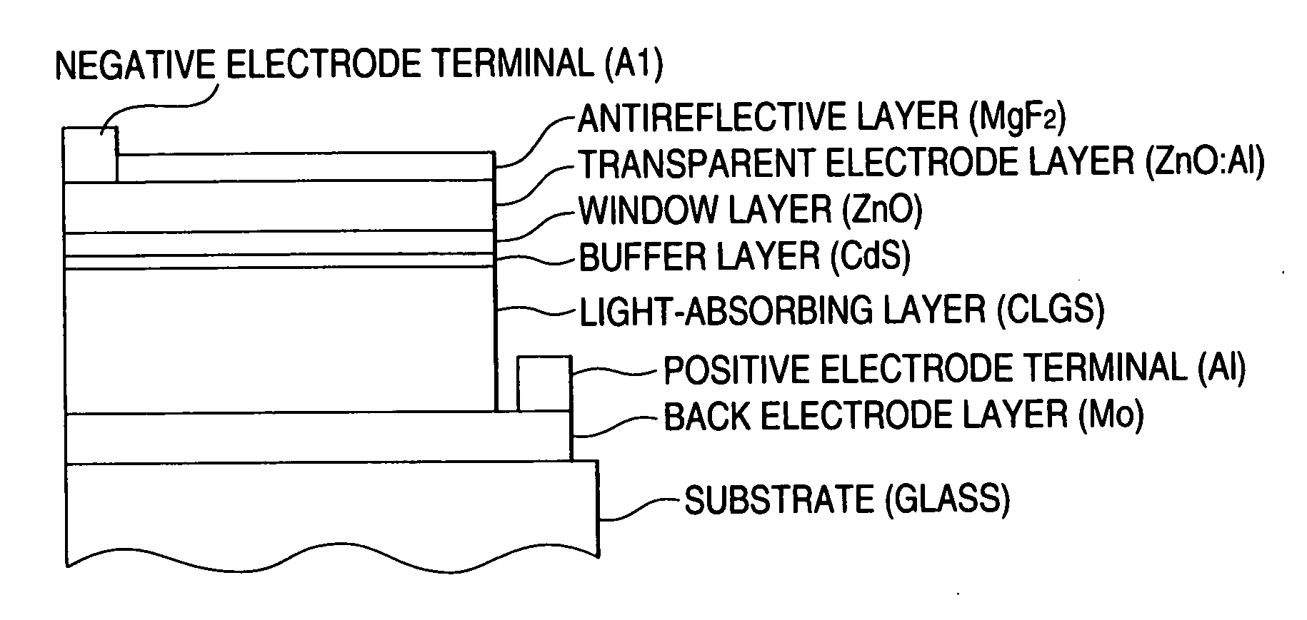
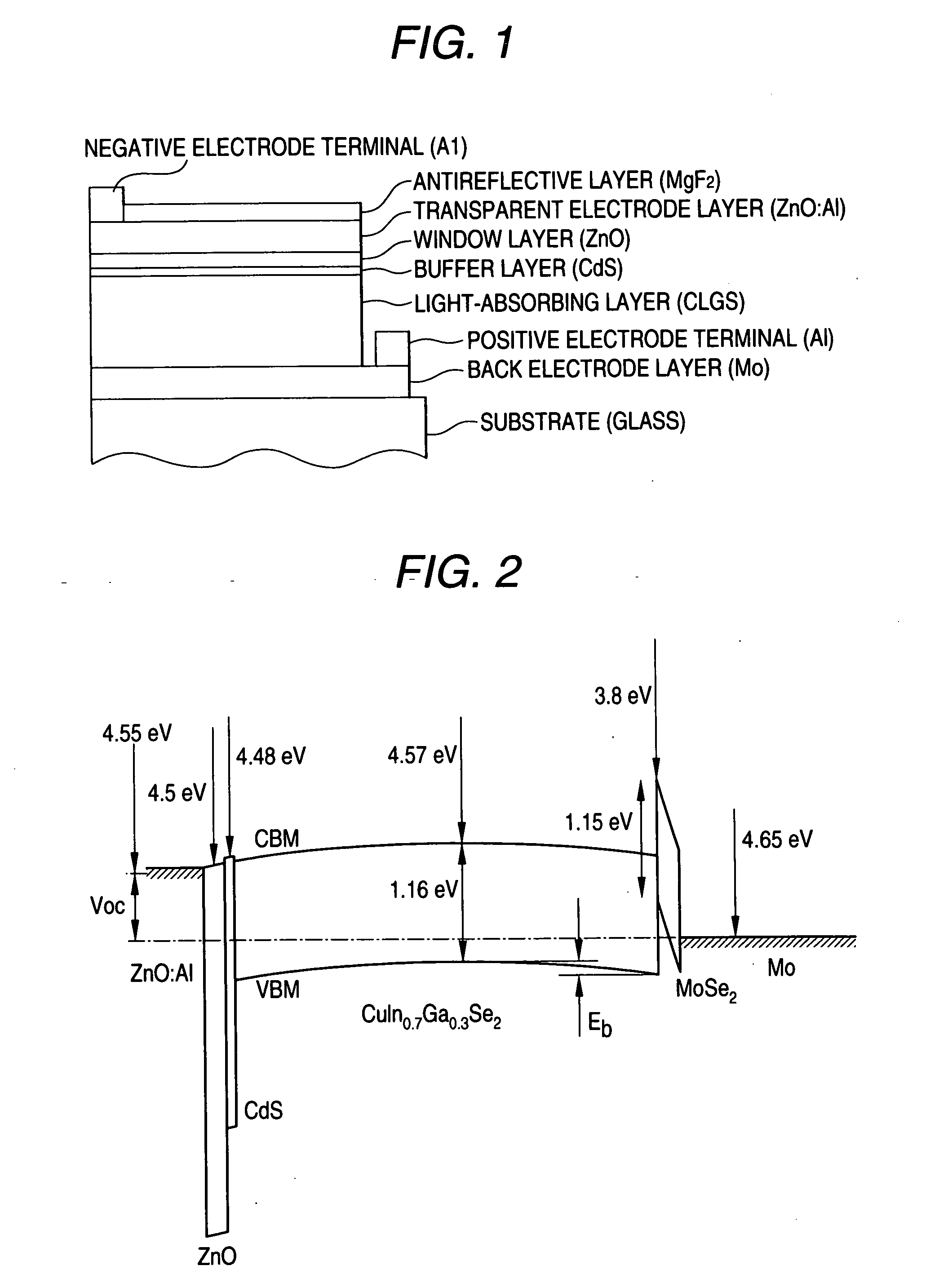
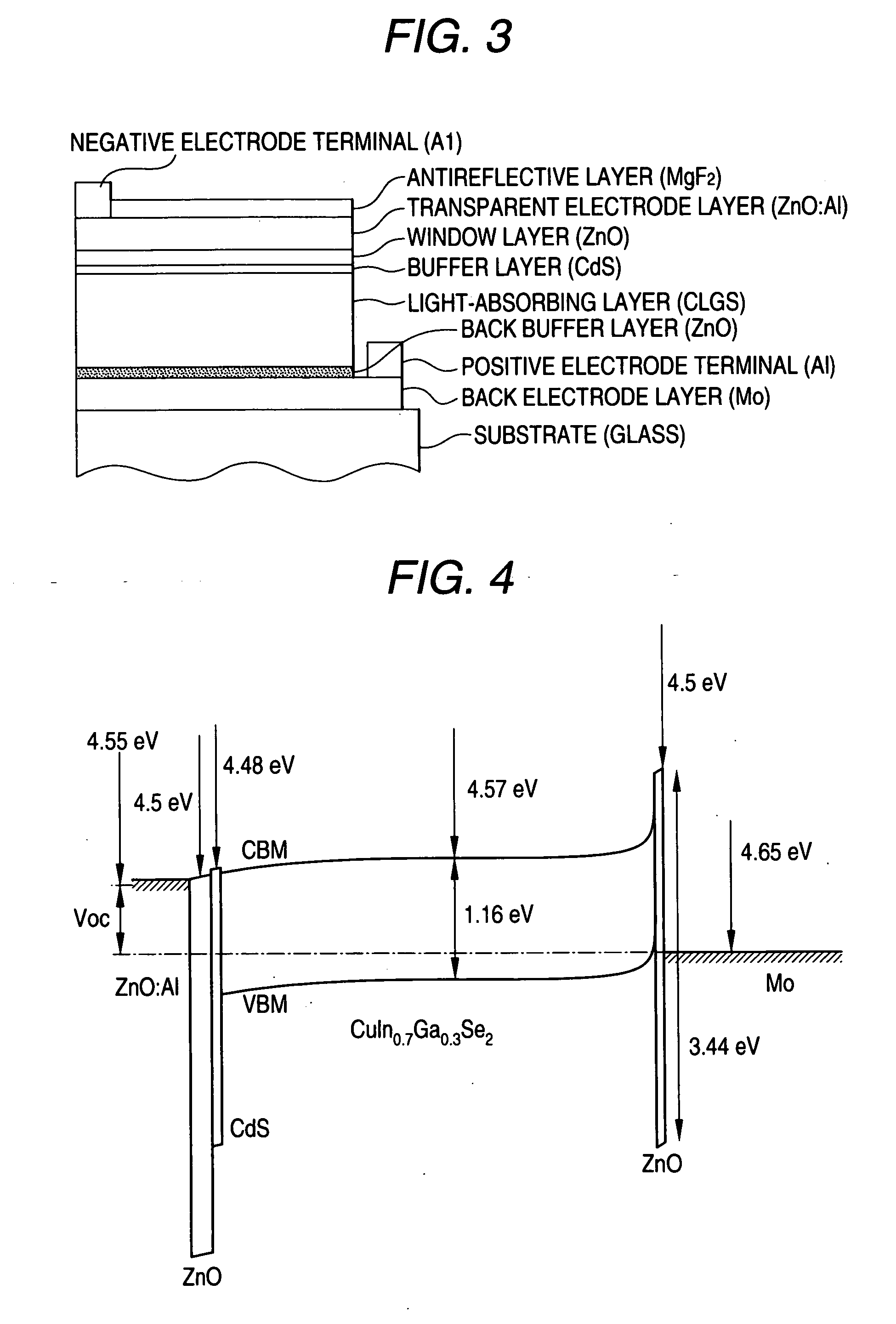
[0052] A layer of Mo as a metal to be a collector electrode is attached on the substrate and, before the formation of the CIGS layer, a p-type ZnO or low carrier concentration n-type back buffer layer is deposited. The other processes may be conducted by conventional methods.

[0053] As a deposition method of p-type ZnO, a pulse laser deposition method (PLD) and a sputtering method using a target containing a suitable precursor are preferable but other means such as vapor deposition and chemical vapor deposition may be employed.

[0054] Those effective for adding to the precursor of the p-type ZnO back buffer layer are PmOn including P2O5, KNO3, K3PO4, K4P2O7, K2SO4, KOH, K2O; K2S, K2Se, NH4NO3, (NH4)3PO4, and the like.

[0055] For deposition of n-type ZnO having a low carrier concentration, vapor deposition by simultaneous irradiation of N is most suitable but the other means may be employed.

[0056] The precursors of N are N2, radicals of N2 and N, NmOn (m, n: an integer), NH3, and th...


PUM


Abstract

A solar cell which comprises a back metal electrode and a light-absorbing layer comprising a p-type CIGS semiconductor on a substrate in this order, wherein the solar cell further comprises a p-type or low carrier concentration n-type semiconductor layer comprising ZnO between the light-absorbing layer and the back metal electrode, and a process for producing the solar cell.

Description

BACKGROUND OF THE INVENTION [0001] 1. Field of the Invention [0002] The present invention relates to a CIGS compound solar cell and a process for producing the same. [0003] 2. Brief Description of the Background Art [0004] A CIGS compound solar cell is a solar cell fundamentally comprising p-type Cu(In1-xGax)Se2 (a mix crystal synthesized from copper indium diselenide and copper gallium diselenide in the ratio of (1−x): x) as a light-absorbing layer and ZnO (zinc oxide) as a window layer. In a solar cell, since a light-absorbing layer plays the most important role for converting light energy into electron / positive hole pairs, the Cu(In1-xGax)Se2 solar cell is called a CIGS solar cell named from the capital letters of the elements forming the material (Cu, In, Ga, and Se). The usefulness of the CIGS solar cell has been already well known and its sale has started. [0005] A cross section of a conventional CIGS solar cell structure is illustratively shown in FIG. 1. The basic constituti...

Claims


Application Information

Patent Timeline
IPC IPC(8): H01L31/00H01L31/0224H01L31/06H01L31/0749H01L31/18
CPCH01L31/022425Y02E10/543Y02E10/541H01L31/0749
Inventor YAMADA, AKIMASATAMPO, HITOSHIMATSUBARA, KOJINIKI, SHIGERUSAKURAI, KEIICHIROISHIZUKA, SHOGOIWATA, KAKUYA
Owner NAT INST OF ADVANCED IND SCI & TECH
Learn More