Photoelectric conversion device

Inactive Publication Date: 2012-12-13
SHARP KK
View PDF2 Cites 1 Cited by
  • Summary
  • Abstract
  • Description
  • Claims
  • Application Information

AI Technical Summary

Benefits of technology

[0013]According to the configuration of the present invention, the plurality of structures and the medium layer satisfy ndie>nmed, and therefore the light delivered to the photoelectric conversion device generates near-field light localized around the structures when the structures are minute. At the same time, the plurality of structures and the medium layer satisfy Dave×nmed/λmax<0.3, and therefore the near-field light around the structures can be absorbed in the photoelectric conversion layer in a concentrated manner. Thus, the conversion efficiency of the photoelectric conversion device is enhanced.
[0014]Some conventional photoelectric conversion devices including a thinned photoelectric conversion layer transmit light to fail to absorb light sufficiently. According to the present invention, in contrast, it is possible to enhance the conversion efficiency of the photoelectric conversion device even with a thi

Problems solved by technology

However, a thinned photoelectric conversion layer transmits therethrough a part of incoming light to result in insufficient light absorption.
A photoelectric conversion device including a thinned photoelectric conversion layer therefore has a reduced optical energy conversion efficiency.
However, conventional solar cells having such rod antennas cannot localize (or concentrate) sunlight to the rod antennas, because the sunlight is supplied into the solar cell by reradiation.
In addition, production of the rod antennas is costly to be likely to hin

Method used


Image

  • Photoelectric conversion device
  • Photoelectric conversion device
  • Photoelectric conversion device

Examples


Example

Embodiment 1

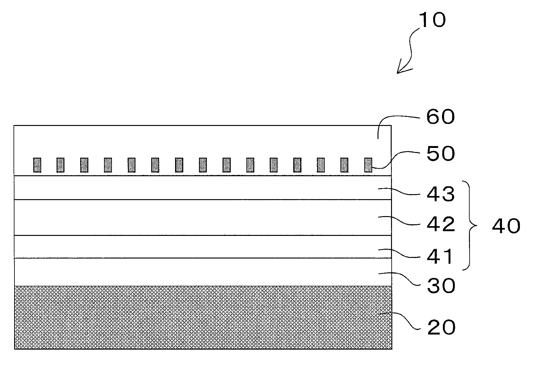
[0050]FIG. 1 is a schematic cross sectional view illustrating a configuration of a solar cell according to Embodiment 1 of the present invention. As illustrated in FIG. 1, a solar cell 10 (photoelectric conversion device) according to the present embodiment comprises a substrate 20, a back surface electrode 30, a photoelectric conversion layer 40, minute dielectrics 50 (structures) and a transparent electrode 60. The photoelectric conversion layer 40, the minute dielectrics 50 (structures) form a photoelectric conversion unit.

[0051]The substrate 20 is a thin plate for supporting other components such as the back surface electrode 30 and the photoelectric conversion layer 40. The substrate 20 is formed of a film of glass or resin, for example. Generally, a glass substrate having a thickness of 3 mm to 5 mm is used. Alternatively, a film may be used to give flexibility. The substrate 20 may be nontransparent as being a plate for supporting the photoelectric conversion laye...

Example

Embodiment 2

[0101]Next, a solar cell according to Embodiment 2 will be described. The solar cell of Embodiment 1 has one photoelectric conversion unit (photoelectric conversion layer 40 and minute dielectrics 50). On the other hand, when a solar cell has a plurality of photoelectric conversion units and the photoelectric conversion units have different maximal sensitivity wavelengths λmax (when a configuration of a so-called tandem solar cell or a so-called multi-junction solar cell is employed), it is possible to achieve a more enhanced photoelectric conversion efficiency of the solar cell. The solar cell according to Embodiment 2 is obtained by applying the above-described configuration of the components including the minute dielectrics 50 to a solar cell having a plurality of photoelectric conversion units. FIG. 10 illustrates the configuration. FIG. 10 is a schematic cross sectional view illustrating the configuration of the solar cell according to Embodiment 2 of the present in...

Example

Embodiment 3

[0110]Next, a solar cell according to Embodiment 3 will be described. Embodiment 1 converts light delivered to the transparent electrode 60 opposite the substrate 20 into electric energy (substrate type). Alternatively, the present invention can be applied to an embodiment that converts light delivered to the substrate into electric energy (superstrate type). FIG. 11 illustrates such an embodiment. FIG. 11 is a schematic cross sectional view illustrating a configuration of the solar cell according to Embodiment 3 of the present invention.

[0111]As illustrated in FIG. 11, a solar cell 210 (photoelectric conversion device) according to the present embodiment comprises a substrate 220, a transparent electrode 230, minute dielectrics 250 (structures), a photoelectric conversion layer 240 and a back surface electrode 260. In Embodiment 3, light is delivered to the substrate side, and therefore the substrate-side electrode is a transparent electrode, and the electrode opposite ...


PUM


Abstract

A photoelectric conversion device comprises a photoelectric conversion layer; a plurality of structures made of a dielectric substance; and a medium layer for transmitting light interposed between the photoelectric conversion layer and the structures or between the structures, or both, wherein the plurality of structures and the medium layer satisfy ndie>nmed and Dave×nmedmax<0.3, wherein λmax is a maximal sensitivity wavelength at which the sensitivity of the photoelectric conversion layer to light energy is maximal, nmed is a refractive index of the medium layer at the wavelength λmax, ndie is a refractive index of the structures at the wavelength λmax, and Dave is an average of shortest distances between an light exposure surface of the photoelectric conversion layer and the structures.

Description

CROSS-REFERENCE TO RELATED APPLICATION[0001]This application is related to Japanese Patent Application No. 2011-128434 filed on Jun. 8, 2011, whose priority is claimed under 35 USC §119, and the disclosure of which is incorporated by reference in its entirety.BACKGROUND OF THE INVENTION[0002]1. Field of the Invention[0003]The present invention relates to a photoelectric conversion device. More particularly, the present invention relates to a solar cell that converts sunlight into electric energy.[0004]2. Description of the Related Art[0005]In recent years, production costs of photoelectric conversion devices have been reduced and, as a result, photoelectric conversion layers in the photoelectric conversion devices have been thinned. However, a thinned photoelectric conversion layer transmits therethrough a part of incoming light to result in insufficient light absorption. A photoelectric conversion device including a thinned photoelectric conversion layer therefore has a reduced opt...

Claims


Application Information

Patent Timeline
IPC IPC(8): H01L31/0232
CPCH01L31/075H01L31/076H01L31/0543Y02E10/548Y02E10/549Y02E10/52
Inventor SATO, TAKANOBUKITAZAWA, TAZUKO
Owner SHARP KK
Why Eureka
Try Eureka