Ramo4 substrate and nitride semiconductor apparatus

Active Publication Date: 2018-11-29
PANASONIC CORP
View PDF0 Cites 0 Cited by
  • Summary
  • Abstract
  • Description
  • Claims
  • Application Information

AI Technical Summary

Benefits of technology

[0011]By use of the RAMO4 substrate of the present disclosure, it is possible to provide a group III nitride semiconductor layer having satisfactory crystallinity and flatness and implement a device having higher performance than that of a group III nitride semiconductor optical device or electronic device produc

Problems solved by technology

However, the sapphire substrate has a large lattice mismatch of 13.8% with group III nitride semiconductors (GaN).
Thus, there is a problem of a high defect density when a group III nitride semiconductor is epitaxially grown on the substrate.
The surface of the ScAlMgO4 substrate cleaved along the (0001) plane aforement

Method used


Image

  • Ramo4 substrate and nitride semiconductor apparatus
  • Ramo4 substrate and nitride semiconductor apparatus
  • Ramo4 substrate and nitride semiconductor apparatus

Examples


embodiment 1

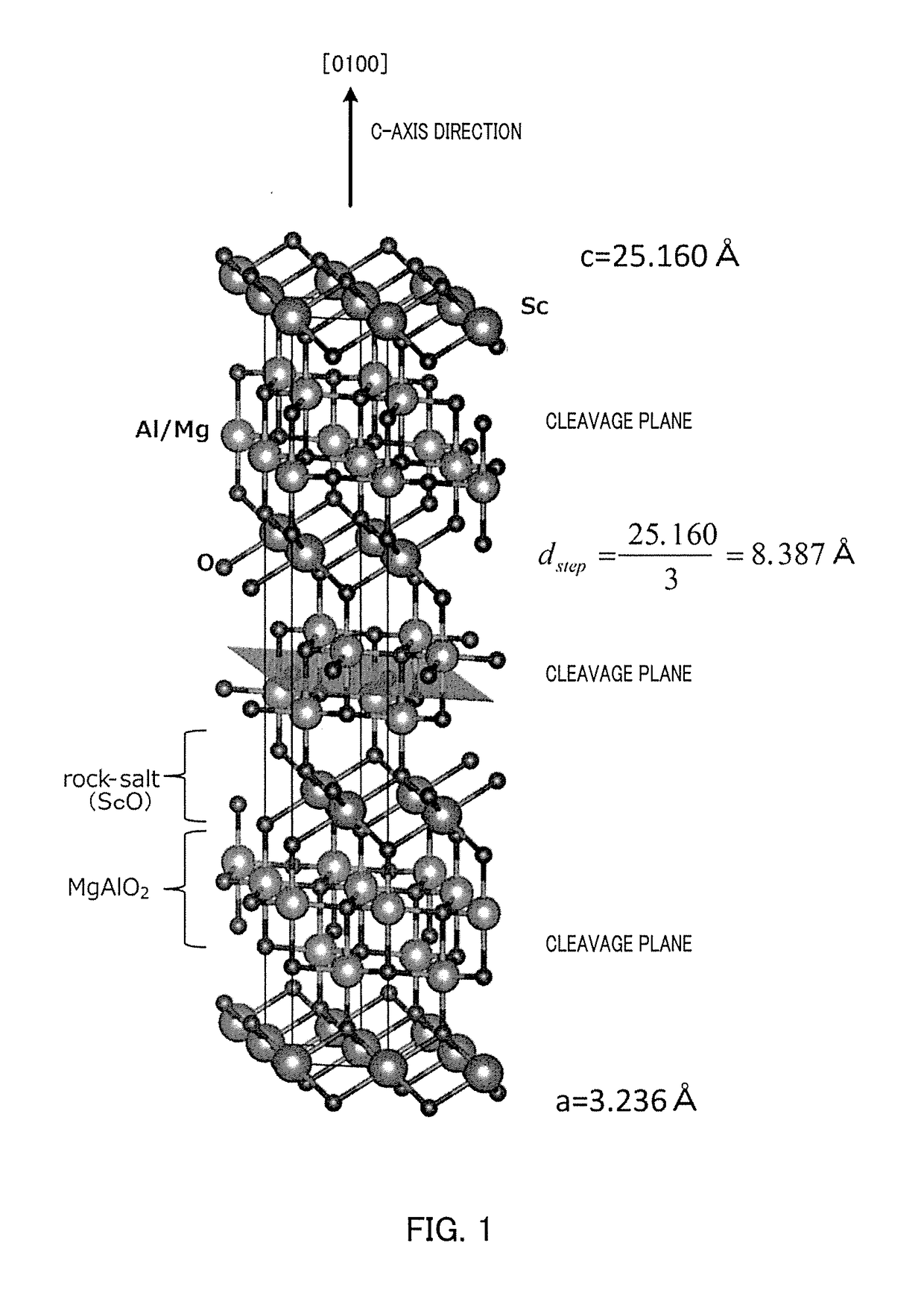
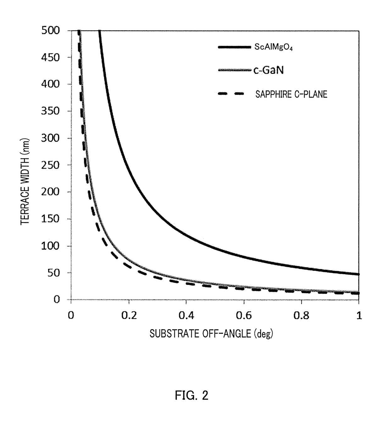
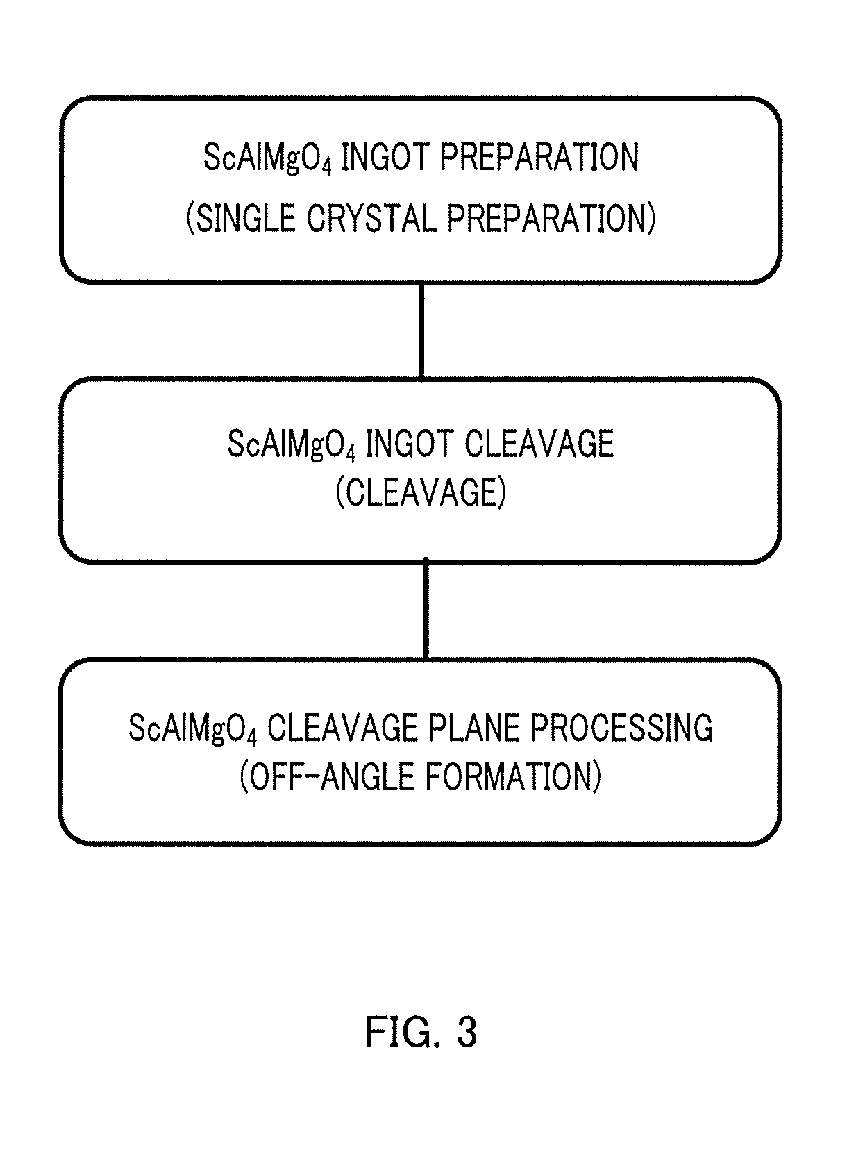
[0028]The crystal structure of ScAlMgO4 is shown in FIG. 1. The crystal of ScAlMgO4 takes a structure in which a MgAlO2 layer as a hexagonal crystal and a ScO layer having a rock salt structure are layered in a [0001] direction (C-axis direction). A (0001) plane (C plane) formed by common cleavage is constituted by a MgAlO2 layer. In the crystal of ScAlMgO4, the crystal lattice constant (c) in the [0001] direction is 25.160 Å, and a step height, which appears by forming an off-angle, will be 25.160 / 3=8.387 Å. This step height is a relatively large value, as compared with the step height (2.593 Å) appearing in a GaN substrate, which is a group III nitride, and the step height (2.165 Å) appearing in a sapphire substrate (C-plane). The step height also influences a length parallel to the (0001) plane of the step (terrace width). As shown in FIG. 2, the ScAlMgO4 crystal, even when allowed to have an off-angle equivalent to that of a GaN substrate or sapphire substrate, will have a surfa...

embodiment 2

[0044]Subsequently, the ScAlMgO4 substrate of Embodiment 2 will be described. In the ScAlMgO4 substrate of the present embodiment, the main plane has an off-angle b (θb) in a direction substantially parallel to the M-plane (1-100) from the C-plane (0001) plane but has no off-angle a, that is, the main plane has an off-angle b tilted θb° with respect to the A-axis direction [11-20] from the C-plane (0001). A method for producing a ScAlMgO4 substrate having such an off-angle b is the same as the method for producing a ScAlMgO4 substrate of Embodiment 1 aforementioned. However, in the aforementioned off-angle formation, the off-direction and the off-angle are adjusted.

[0045]The preferable range of the off-angle b in the ScAlMgO4 substrate of the present embodiment is 0.05°≤|θb|≤0.4°, more preferably 0.1°≤|θb|≤0.4°, still more preferably 0.1°≤|θb|≤0.4°. Hereinbelow, the reason will be described.

[0046]As in Embodiment 1, a group III nitride semiconductor layer (GaN film) was epitaxially ...

embodiment 3

[0047]Subsequently, the ScAlMgO4 substrate of Embodiment 3 will be described. In the ScAlMgO4 substrate of the present embodiment, the main plane is tilted θa° with respect to the M-axis direction and θb° with respect to the A-axis direction, from the C-plane (0001 plane). That is, the substrate includes the compound off-angle of the off-angle a and the off-angle b. A method for producing a ScAlMgO4 substrate having such an off-angle a and an off-angle b is the same as in Embodiment 1 aforementioned. However, in the aforementioned off-angle formation, the off-direction and the off-angle are adjusted.

[0048]In the ScAlMgO4 substrate of the present embodiment, the range of the off-angle a is preferably 0.05°≤|θa|≤0.8°, more preferably 0.2°≤|θa|≤0.6°. The range of the off-angle b is preferably 0.05°≤|θb|≤0.4°, more preferably 0.1°≤|θb|≤0.4°, still more preferably 0.1°≤|θa|<0.4°. Hereinbelow, the reason will be described.

[0049]As in Embodiment 1, group III nitride semiconductor layer (Ga...


PUM


Abstract

An RAMO4 substrate including a single crystal represented by a general formula RAMO4, wherein R represents one or more trivalent elements selected from a group consisting of Sc, In, Y, and lanthanide elements, A represents one or more trivalent elements selected from a group consisting of Fe(III), Ga, and Al, and M represents one or more divalent elements selected from the group consisting of Mg, Mn, Fe(II), Co, Cu, Zn, and Cd, in which a main plane of the RAMO4 substrate has an off-angle a tilted θa° with respect to an M-axis direction from a C-plane and 0.05°≤|θa|≤0.8° is satisfied.

Description

CROSS REFERENCE TO RELATED APPLICATIONS[0001]This application is entitled to and claims the benefit of Japanese Patent Application No. 2017-102862, filed on May 24, 2017, the disclosure of which including the specification, drawings and abstract is incorporated herein by reference in its entirety.TECHNICAL FIELD[0002]The present disclosure relates to an RAMO4 substrate and a group III nitride semiconductor apparatus.BACKGROUND ART[0003]Group III nitride semiconductors, which cover a wide band gap by means of combinations of group III elements such as Ga, Al, and In, are widely used in optical semiconductor devices such as light emitting diodes (LEDs) and laser diodes (LDs) and electronic devices for high frequency and high-power applications. These group III nitride semiconductor-containing devices are generally produced by epitaxially growing a group III nitride semiconductor layer on a sapphire substrate. However, the sapphire substrate has a large lattice mismatch of 13.8% with g...

Claims


Application Information

Patent Timeline
IPC IPC(8): H01L33/00H01L21/02H01L29/20H01S5/22
CPCH01L33/007H01L21/0242H01L29/2003H01L21/0254H01S5/2216C30B15/00C30B25/18C30B29/22C30B29/403C30B29/406H01L33/16H01L21/02433H01L21/02458H01L21/0262C30B15/36C30B25/183C30B25/186
Inventor UETA, AKIO
Owner PANASONIC CORP
Why Eureka
Try Eureka