
Photon/energy identifying x-ray and gamma ray imaging device ("pid") with a two dimensional array of pixels and system therefrom

a technology pid, which is applied in the field of x-ray and gamma ray imaging, can solve the problems of affecting the performance of the cmos and the detector which is connected to the cmos, generating a lot of heat, and unable to accommodate more than few counters on each pixel, so as to reduce the amount of data and event rate, the effect of significantly reducing the drawbacks

Active Publication Date: 2012-11-08
OY AJAT LTD
View PDF11 Cites 35 Cited by
  • Summary
  • Abstract
  • Description
  • Claims
  • Application Information

AI Technical Summary

Benefits of technology

[0014]The current invention reduces significantly or mitigates the drawbacks of the prior art. In accordance with the present invention there is provided for an imaging device comprising an array of imaging pixels, each pixel having an input amplifier for receiving and amplifying the electronic signal generated in response to incident single x-ray events, circuitry for reading out the single photon signal (for example voltage peak-hold value or current), circuitry for digitizing the individual x-ray event signal outside each pixel and processing such for recording its energy and displaying it for imaging selectively and according to the energy. The current invention teaches digital buffers inside each pixel for temporary storage of event / signal information and / or also a digital controller off pixel for reducing the amount of data and event rate in either time or space or both, thus rendering the readout and use of this photon identifying imaging device practical.
[0021]The digital controller contains Digital Processing Units (“DPU”), capable of reducing the amount of data either time wise, or spatial wise or both and rendering the readout sequence practical. Time wise data reduction comprises integrating (or summing) the data over a period of time, which is called a readout frame and providing the number of photons events above a certain threshold for every pixel and every frame. Spatial data reduction comprises combining M×N detector pixels to a super pixel and providing the number of incident photons for each of M×N energy bins for each super pixel.

Problems solved by technology

Even with the most advanced CMOS processes, one cannot accommodate (cannot fit) more than few counters on each pixel.
This in turn generates a lot of heat, which affects the performance of the CMOS and the detector which is connected to the CMOS.
Energy resolution suffers and electronic noise increases.
Active cooling becomes necessary increasing cost and complexity.Digital electronics and particularly counters on each pixel are very difficult to shield from the analog (amplifier) electronics.
Although such shielding techniques exist to those that exert in this field, in practical terms, such counters can couple with the analog electronics and cause noise.

Method used


Image

  • Photon/energy identifying x-ray and gamma ray imaging device ("pid") with a two dimensional array of pixels and system therefrom
  • Photon/energy identifying x-ray and gamma ray imaging device ("pid") with a two dimensional array of pixels and system therefrom
  • Photon/energy identifying x-ray and gamma ray imaging device ("pid") with a two dimensional array of pixels and system therefrom

Examples


Embodiment Construction

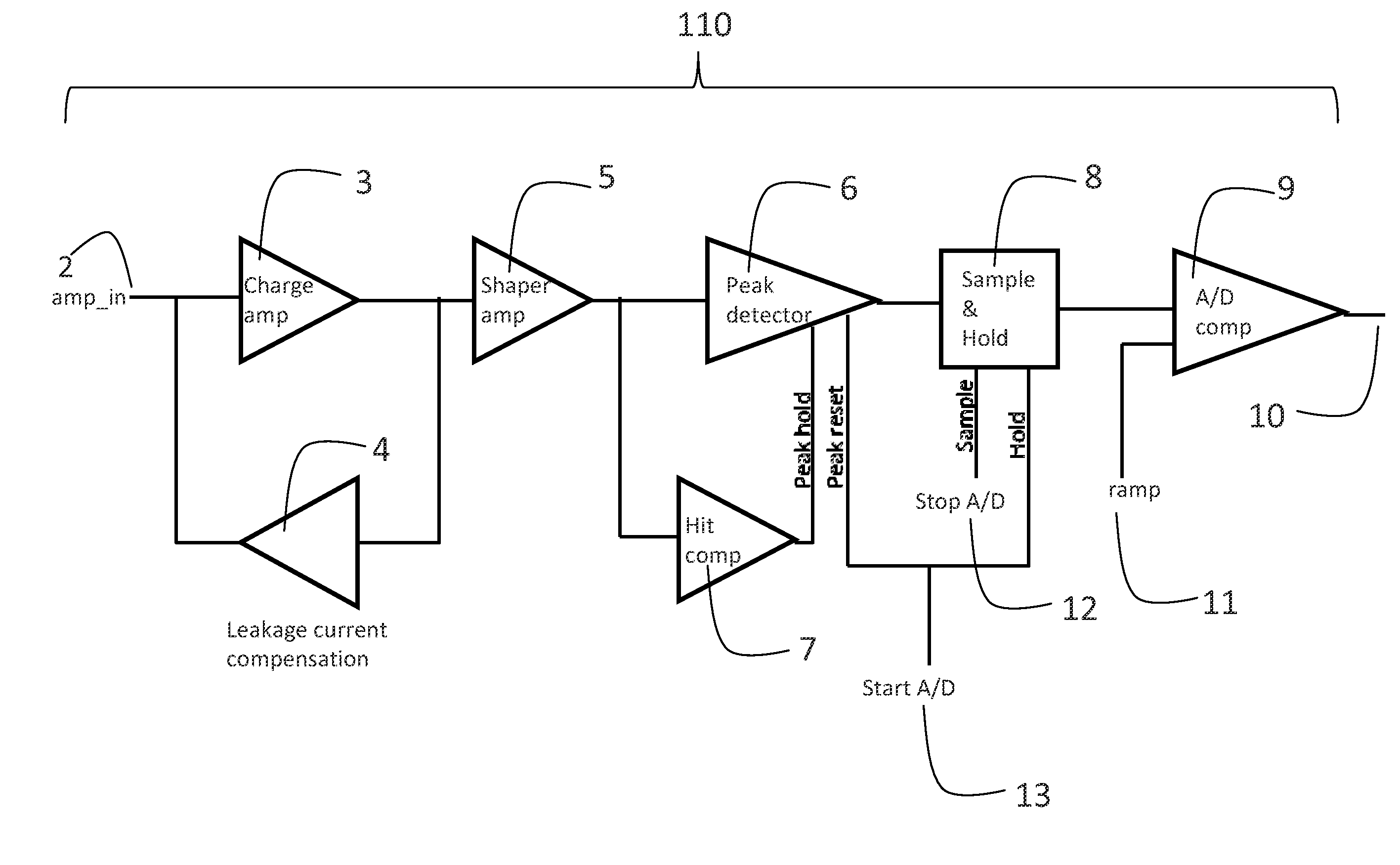
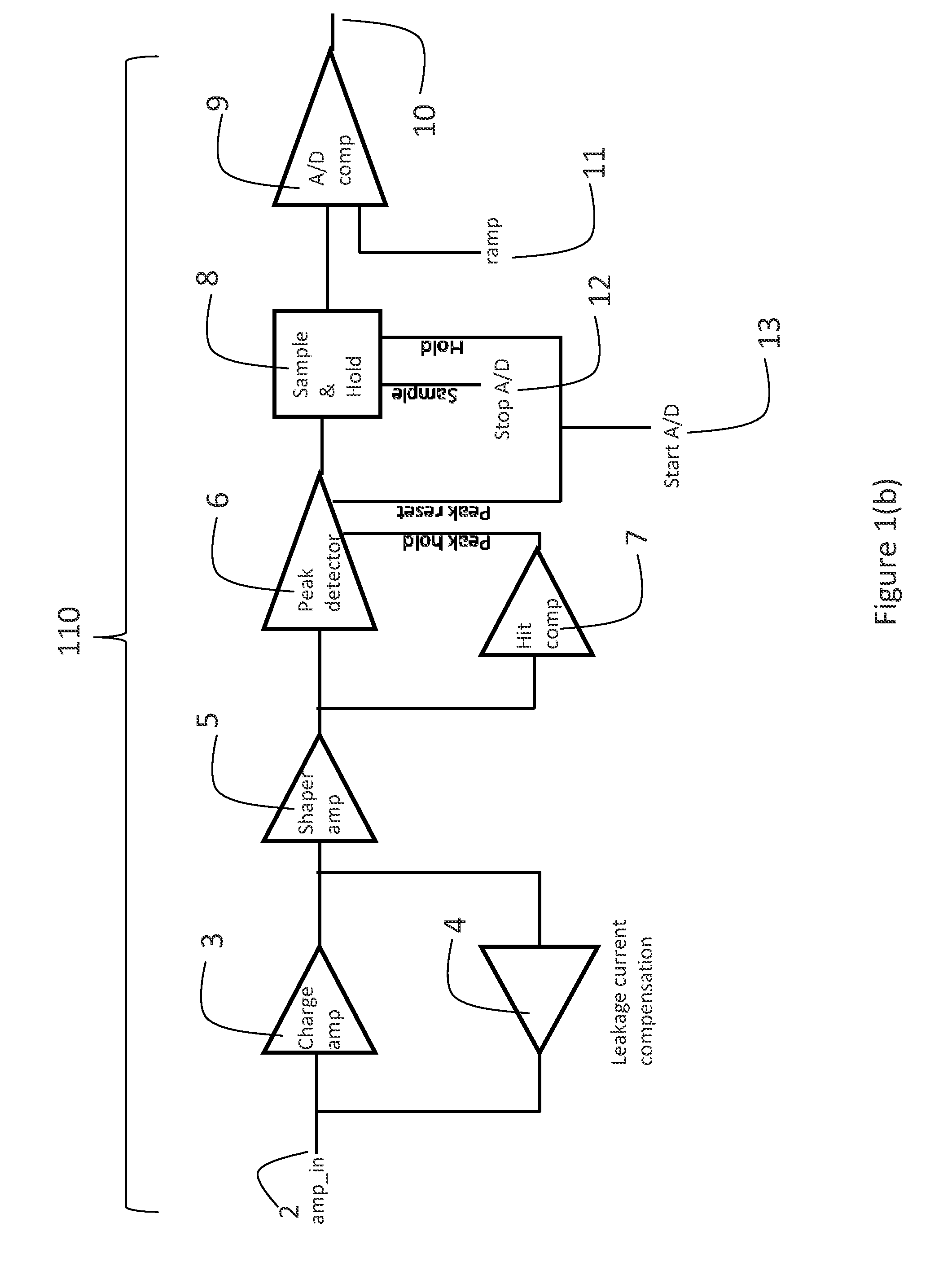
[0033]With reference to FIGS. 1(a), 1(b), 1(c), and 2, the invention includes a radiation imaging device 32 having a detector substrate 27 connected to the readout substrate 25 and further substrate 28.

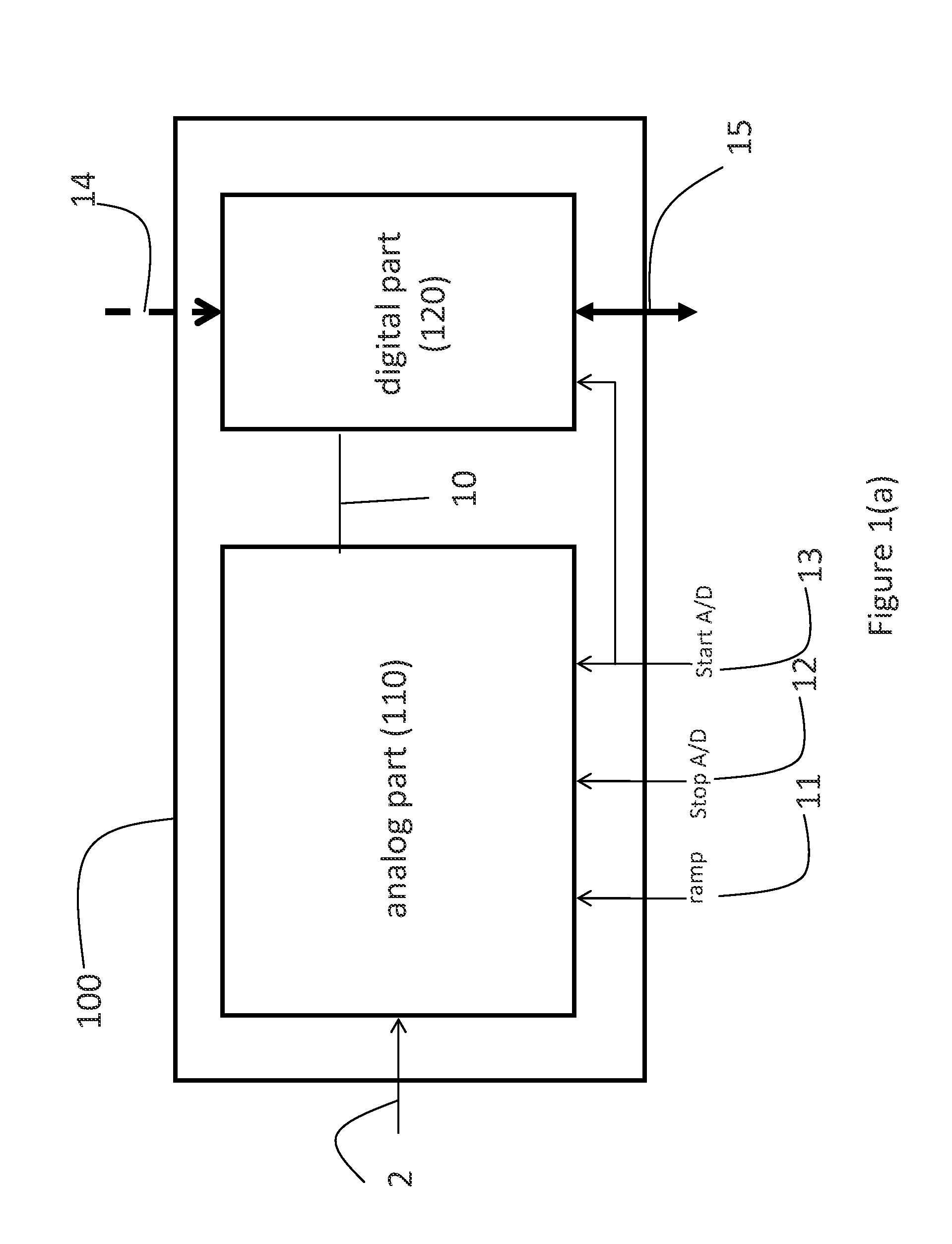
[0034]A block diagram of the pixel cell circuit 100 of a preferred embodiment of the present invention is shown in FIG. 1a. Preferably there is one pixel cell circuit 100 associated with each detector pixel, but other embodiments are possible, for example several detector pixels corresponding to the same pixel cell circuit 100 or vice versa.

[0035]FIG. 2 shows an overview of the inventive radiation imaging device 32.

[0036]A radiation imaging detector 32 (an image sensor) is comprised of imaging cells 23, i.e., plural detector pixels implemented on detector substrate 27 and connected via bump-bonds 26 to the readout substrate 25. Other types of connection are possible such as using conductive epoxy, wire bonding or epitaxially growing the detector on the readout substrate. The readout s...


PUM


Abstract

An photon (energy) identifying radiation imaging device, for imaging x-ray, gamma ray and charged radiation in medical, dental and industrial applications. The imaging device includes a detector substrate and a readout substrate. The detector substrate has a plurality of detector pixels and the readout substrate has a plurality of corresponding pixel readout circuits. Each pixel readout circuit has circuitry for processing an input analog signal and also has one or more buffers for temporarily storing values corresponding to the signal of at least two individual incoming radiation events. The readout substrate includes a digital controller having digital processing units for carrying out off-pixel digital signal processing and data / rate reduction prior to readout.

Description

RELATED APPLICATIONS[0001]This application claims priority to U.S. Provisional Application 61 / 482,381 filed May 4, 2011.BACKGROUND OF THE INVENTION[0002]The current invention generally relates to the field of x-ray and gamma ray imaging and more specifically to an imaging device used for collecting photons within a certain energy range or energy bins. Most often such imaging devices are referred to as “photon counting” devices and consist of a two dimensional array of pixels, each pixel comprising a detector element produced with lithography semiconductor techniques on a monolithic detector substrate for converting x / gamma rays into an electronic signal and a circuit element connected to the detector element for counting the incident x / gamma rays within a given energy range or several energy bins, utilizing in-pixel counters (thus the expression “photon counting”), or in other words counters for counting plural photons, such counters residing on each individual pixel circuit and for...

Claims


Application Information

Patent Timeline
Patent Type & Authority Applications(United States)
IPC IPC(8): G01T1/20H01L27/146G01T1/24
CPCG01T1/247H04N5/32H04N5/378H04N5/3745H04N5/347H04N25/46H04N25/77H04N23/30H04N25/773G01T1/24A61B6/00G01T1/2928A61B6/4241H04N25/75
Inventor SPARTIOTIS, KONSTANTINOSPANTSAR, TUOMASLAMBROPOULOS, CHARALAMPOSORPHANOUDAKIS, THEOFANIS
Owner OY AJAT LTD
Learn More