Photoplating of metal electrodes for solar cells

a metal electrode and solar cell technology, applied in the direction of electrolysis process, semiconductor devices, electrolysis components, etc., can solve the problems of poor adhesion and contact resistance between the plated metal and the semiconductor surface, the difficulty of plating to nucleate at other locations of the semiconductor surface, and the polarity of silicon being plated with the same metal type. , to achieve the effect of illuminating the photovoltaic devi

Inactive Publication Date: 2012-11-08
NEWSOUTH INNOVATIONS PTY LTD
View PDF2 Cites 1 Cited by
  • Summary
  • Abstract
  • Description
  • Claims
  • Application Information

AI Technical Summary

Benefits of technology

[0008]b) illuminating the photovoltaic device, using a light source of time varying intensity, whereby nett plating is

Problems solved by technology

One common problem with metal contacts formed to solar cell surfaces via these techniques is that the plating solutions have a high density of metal ions such that, when plating the metal nucleates at a particular site on the semiconductor surface, and that location then becomes the preferable site for continuing rapid plating which is fed from the high concentration of metal ions available in the solution.
Unfortunately the already plated surface provides the most attractive site for further metal ion deposition making it difficult for plating to nucleate at other locations of the semiconductor surface.
The result is relatively poor adhesion and contact resistance between the plated metal and the semiconductor surface.
Another common problem of prior. plating techniques is that they often lead to both polarities of silicon being plated with the same type of metal, rather than allowing the use of the most desirable metal for each contact.
As

Method used


Image

  • Photoplating of metal electrodes for solar cells
  • Photoplating of metal electrodes for solar cells
  • Photoplating of metal electrodes for solar cells

Examples


Embodiment Construction

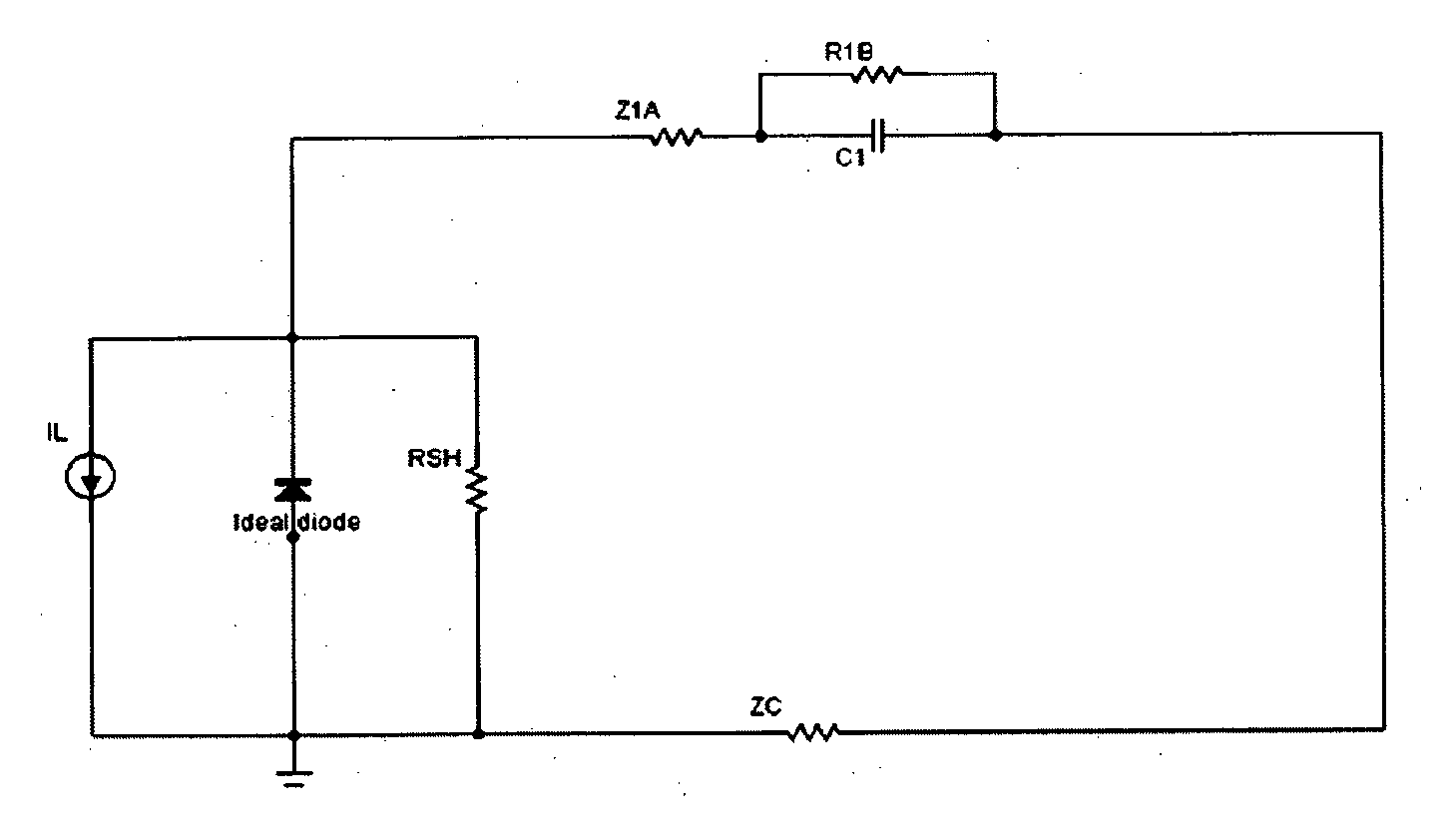
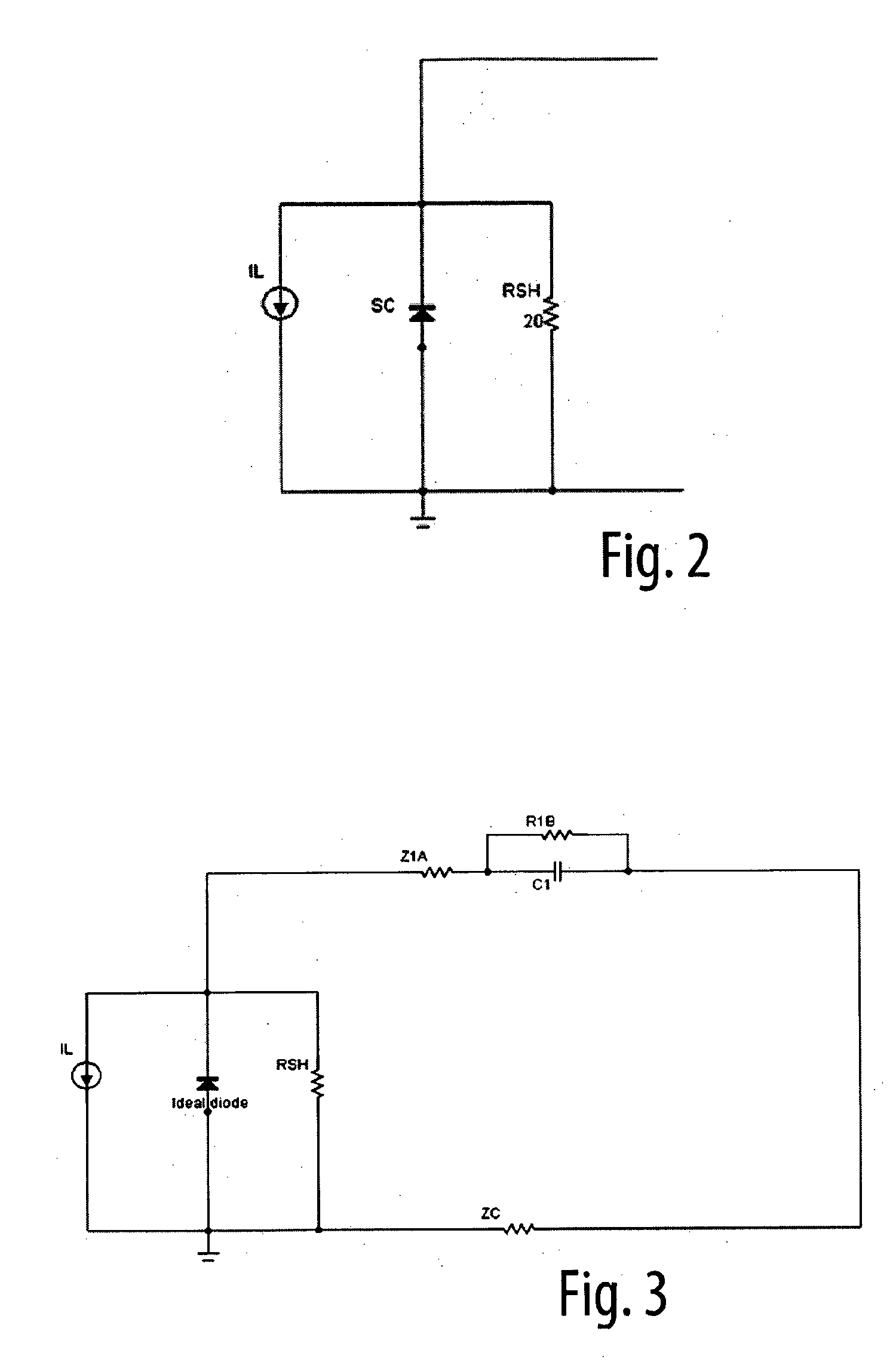
[0032]New approaches for the plating of contacts on solar cells are described herein based on light induced plating (LIP) methods which ameliorate some or all of the difficulties experienced with prior methods. Excellent adhesion may be obtained between the plated metal and the semiconductor surface while high aspect ratios for the metallisation may also be achieved through producing average plating rates in the direction perpendicular to the semiconductor surface that may be up to four times greater than the plating rates parallel to the surface that cause widening of the lines. These approaches may also allow different metals to be used on contacts to different polarity semiconductors while simultaneously avoiding corrosion of either metal contact during the plating process. It is also possible with these approaches to avoid the need for external power sources or any external electrodes to contact the solar cell.

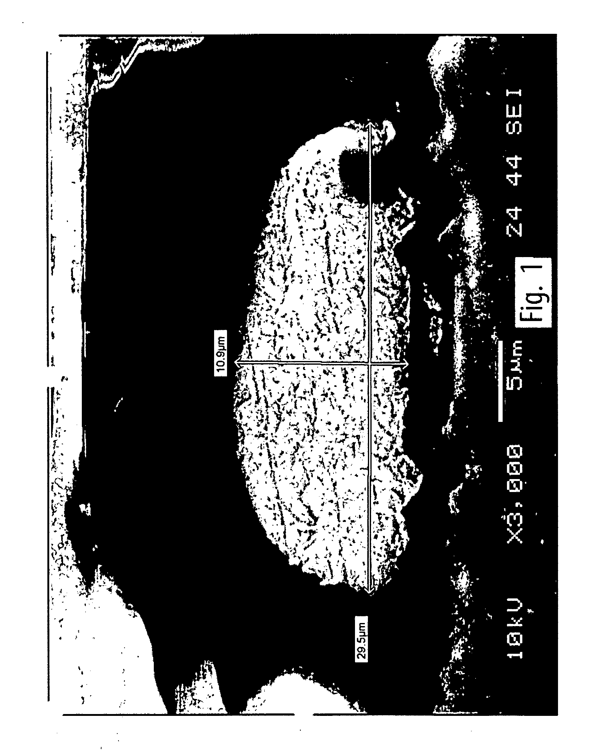
[0033]To understand the LIP process, the following example uses a cop...


PUM


Abstract

A method of photoplating a metal contact onto a surface of a cathode of a photovoltaic device is provided using light induced plating technique. The method comprises: a) immersing the photovoltaic device in a solution of metal ions, where the metal ions are a species which is to be plated onto the surface of the cathode of the photovoltaic device; and b) illuminating the photovoltaic device, using a light source of time varying intensity. This results in nett plating which is faster in a direction normal to the surface of the cathode than in a direction in a plane of the surface of the cathode.

Description

INTRODUCTION[0001]The present invention relates generally to the manufacture of photovoltaic devices and in particular the invention provides improvements to metal plating methods for contact formation and their use in photovoltaic device manufacture which by way of example will be described with reference to solar cell manufacture.BACKGROUND[0002]Solar cells in general require two metal contacts to the semiconductor material, one of each polarity, to allow light generated charge from within the solar cell to be extracted and allowed to flow in external electrical wires as electricity. Most solar cells have one polarity of contact on the top surface and the opposite polarity metal contact on the rear surface. For example, in general, silicon solar cells have different metals for the front and rear contacts due to the different requirements when contacting n-type and p-type silicon. In addition, other attributes of the metal such as its electrical conductivity and thermal expansion c...

Claims


Application Information

Patent Timeline
IPC IPC(8): H01L31/18
CPCC25D5/18H01L31/022425Y02E10/50C25D5/006C25D7/126C25D17/001C25D5/011
Inventor MAI, LYMAREE WENHAM, ALISONROSS WENHAM, STUART
Owner NEWSOUTH INNOVATIONS PTY LTD
Why Eureka
Try Eureka