Method for making semi-conductor nanocrystals

a technology of semi-conductor nanocrystals and nanocrystals, which is applied in the direction of material nanotechnology, semiconductor devices, electrical devices, etc., can solve the problems that the dimensions of these nanocrystals are too large to be used in some nano-scale electronic devices

Inactive Publication Date: 2012-11-08
COMMISSARIAT A LENERGIE ATOMIQUE ET AUX ENERGIES ALTERNATIVES +1
View PDF1 Cites 2 Cited by
  • Summary
  • Abstract
  • Description
  • Claims
  • Application Information

AI Technical Summary

Problems solved by technology

The dimensions of these nanocrystals however are too large to be used in some nanoscale electronic devices,

Method used


Image

  • Method for making semi-conductor nanocrystals
  • Method for making semi-conductor nanocrystals
  • Method for making semi-conductor nanocrystals

Examples


first embodiment

[0035]The steps of a method for making semi-conductor nanocrystals are described in connection with FIGS. 1 and 2.

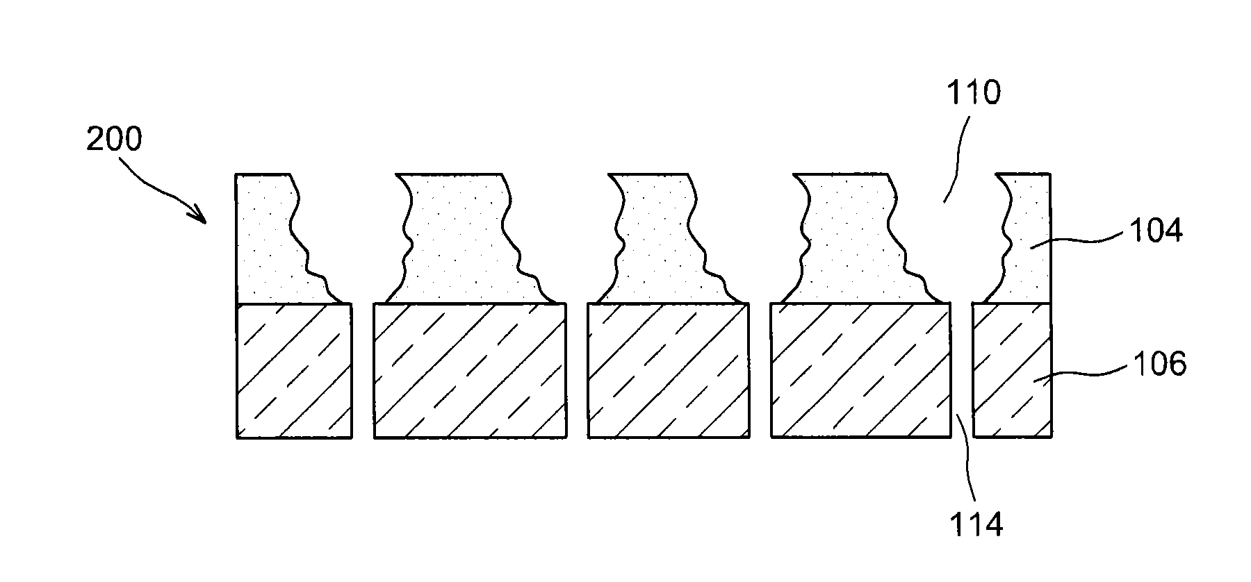
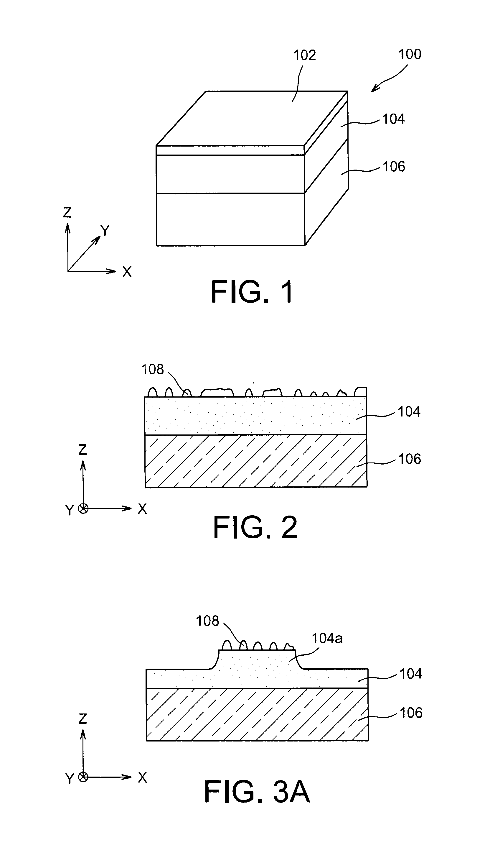
[0036]The method for making semi-conductor nanocrystals is implemented from a first SOI substrate 100 (represented in FIG. 1) comprising a thin layer (having a thickness lower or equal to about 1 μm, and preferably between about 1 nm and 100 nm), of monocrystalline silicon 102, having a crystallographic orientation (001), covering a buried dielectric layer 104 comprising SiO2 which rests on a monocrystalline silicon thick layer 106 forming the layer supporting the SOI substrate.

[0037]The method is also implemented for a second, third and fourth SOI substrate, having similar structures to that of the first SOI substrate 100, but wherein the silicon thin layer 102 is composed of silicon called biaxially stressed in the plane of the layer 102, that is in both directions X and Y represented in FIG. 1. This biaxial stressed condition is equivalent to a biaxial strain undergo...

second embodiment

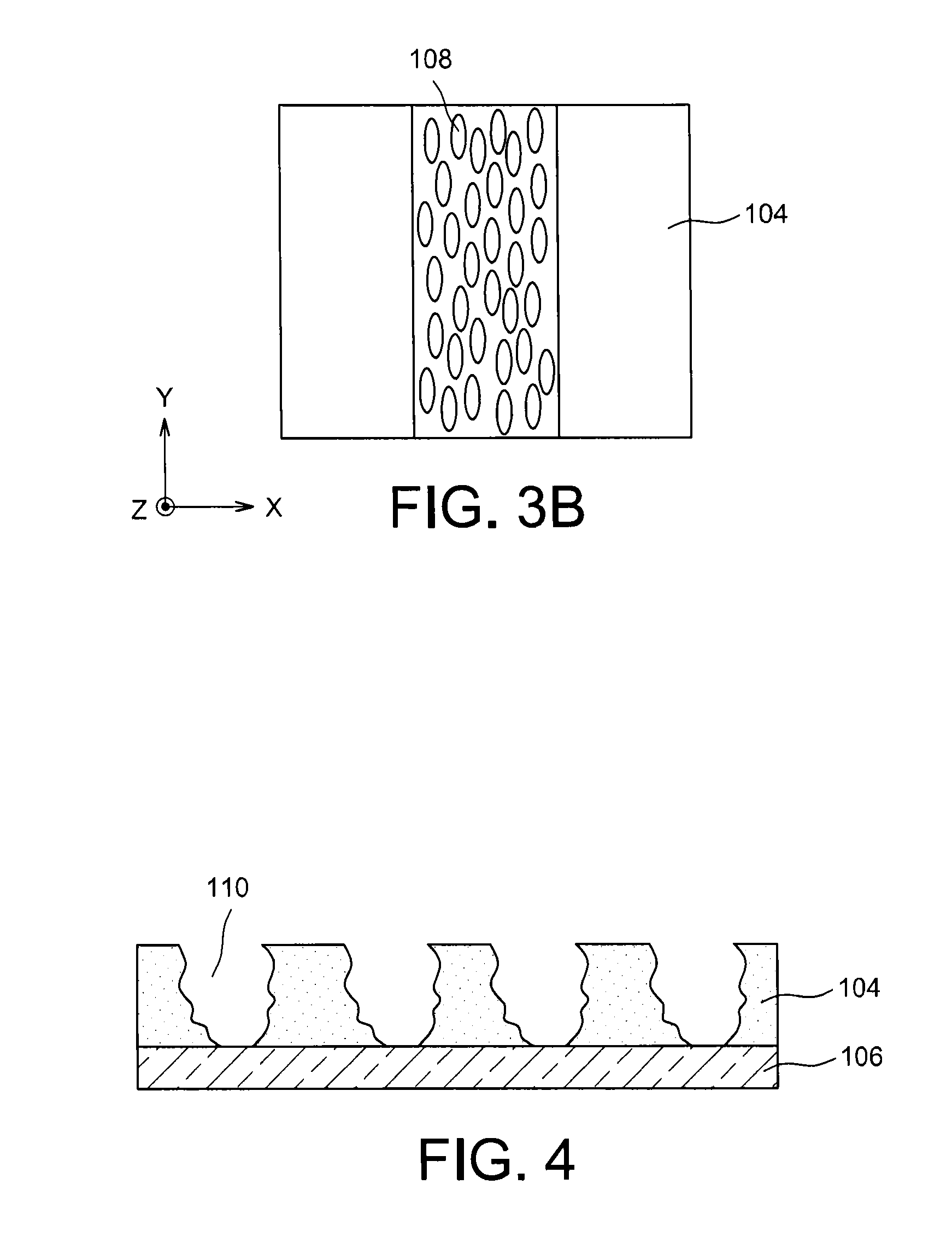
[0059]In a second embodiment, the step of chemically treating the silicon thin layer 102 can be replaced by depositing carbon chemical species, forming on at least one part of the thin layer 102 a carbon layer the thickness of which will be selected as a function of the desired density of the silicon nanocrystals, as well as a function of the desired dimensions of theses silicon nanocrystals.

[0060]The carbon layer is formed by exposing, or irradiating, the silicon thin layer 102 by an electron beam for a duration proportional to the desired carbon thickness. The carbon is locally deposited in order to define, at the surface of the thin layer 102, a polluted surface whereas its environment is not or few polluted. The carbon making up the layer formed by exposing the semi-conductor thin layer 102 comes from the environmental pollution surrounding the substrate, and corresponds for example to the environmental pollution within a scanning electron microscope. The electron beam has for e...


PUM


Abstract

A method for making semi-conductor nanocrystals, including at least the steps of:
    • forming solid carbon chemical species on a semi-conductor thin layer provided on at least one dielectric layer, the dimensions and the density of the carbon chemical species formed on the semi-conductor thin layer being a function of the desired dimensions and density of the semi-conductor nanocrystals;
    • annealing the semi-conductor thin layer, performing a dewetting of the semi-conductor and forming, on the dielectric layer, the semi-conductor nanocrystals.

Description

TECHNICAL FIELD[0001]The invention relates to a method for making semi-conductor nanocrystals obtained by dewetting a semi-conductor thin layer provided on a dielectric layer, and which can be used for making microelectronic and / or nanoelectronic devices, for example memory devices or LED type light emissive devices.[0002]The invention also relates to a method for making a porous dielectric layer resorting to semi-conductor nanocrystals.[0003]The invention also relates to a method for making semi-conductor nanocrystals accurately positioned in the thickness of a stack of layers comprising at least one dielectric material.STATE OF PRIOR ART[0004]For making semi-conductor nanocrystals, that is semi-conductor aggregates the dimensions of which can be between about a few nanometres and a few hundred nanometres, it is known to make a dewetting of a silicon thin layer provided on a SiO2 layer. Indeed, when the silicon thin layer, forming for example the active layer, or upper layer, of a ...

Claims


Application Information

Patent Timeline
IPC IPC(8): H01L21/20B82Y40/00
CPCB82Y10/00B82Y40/00H01L21/02381H01L21/02488H01L21/02529H01L21/02532B82Y30/00H01L21/02601H01L21/02667H01L29/0665H01L29/66075H01L29/7613H01L21/0259
Inventor BOROWIK, LUKASZBARBE, JEAN-CHARLESBUSSMANN, EZRACHEYNIS, FABIENLEROY, FRÉDÉRICMARIOLLE, DENISMÜLLER, PIERRE
Owner COMMISSARIAT A LENERGIE ATOMIQUE ET AUX ENERGIES ALTERNATIVES
Why Eureka
Try Eureka