

Semiconductor device
- Summary
- Abstract
- Description
- Claims
- Application Information
AI Technical Summary
Benefits of technology
Problems solved by technology
Method used
Image

Examples
embodiment 1
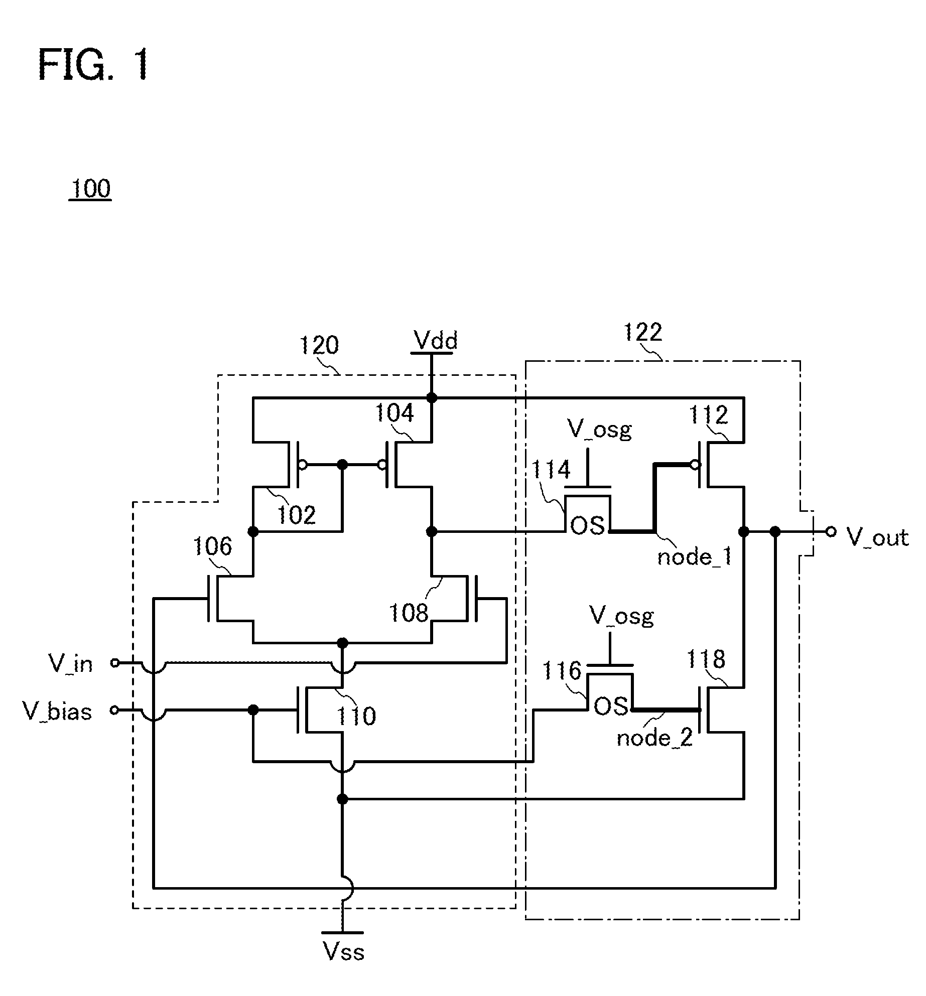
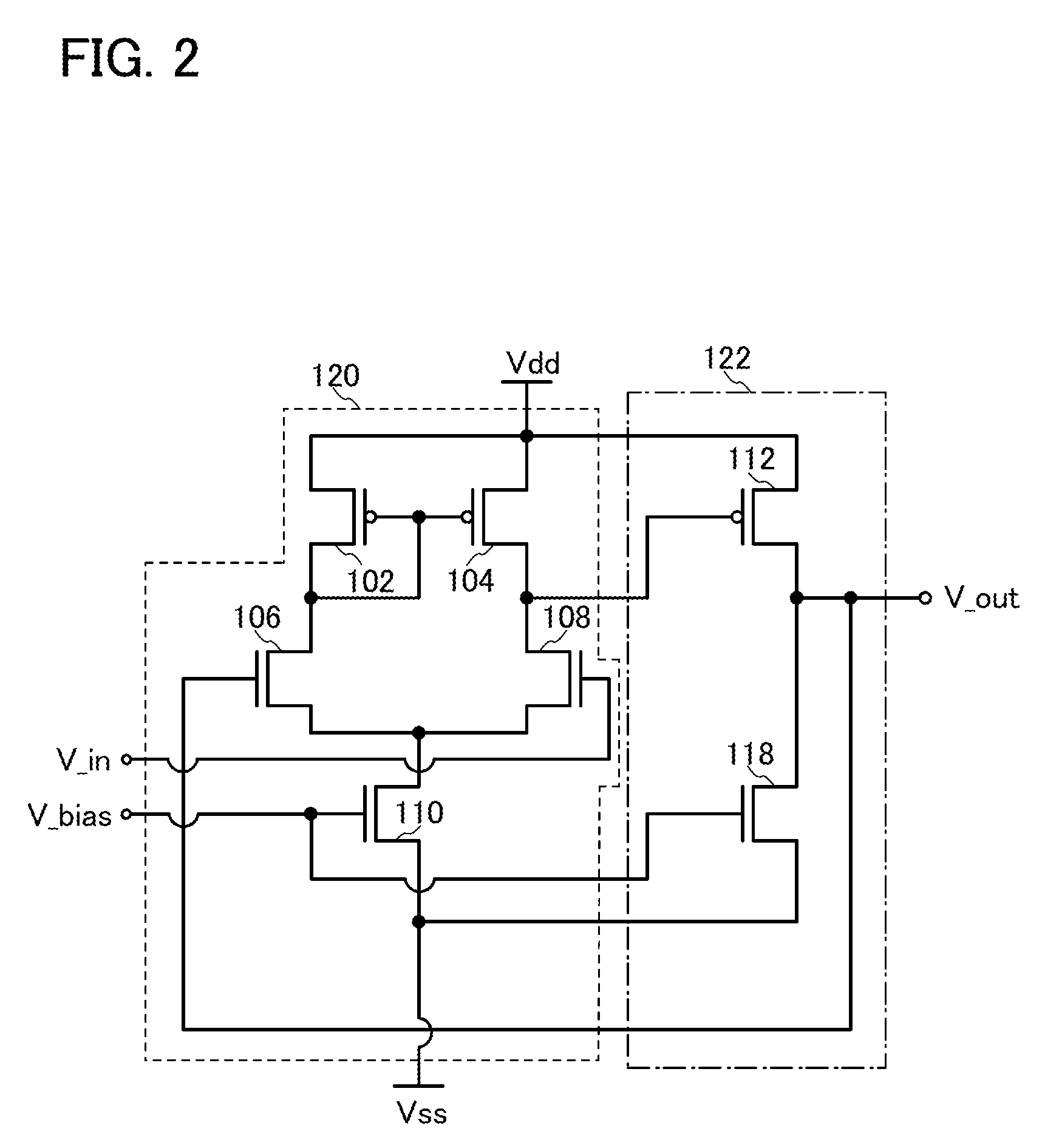
[0046]In this embodiment, a semiconductor device according to one embodiment of the present invention will be described. FIGS. 23A and 23B are schematic diagrams illustrating a semiconductor device according to one embodiment of the present invention.
[0047]A semiconductor device illustrated in FIG. 23A includes a differential amplifier 12 in which a first input terminal to which an input potential V—in is input and a second input terminal to which a reference potential V—bias is input are electrically connected to each other and a gain stage 14 which includes at least a first transistor 16, a second transistor 18, a third transistor 20, and a fourth transistor 22 and is electrically connected to an output terminal from which an output potential V—out is output. The differential amplifier 12 is electrically connected to power supply potential lines Vdd and Vss. A first terminal of the first transistor 16 is electrically connected to the first input terminal through the differential a...
embodiment 2
[0086]In this embodiment, a configuration example of the semiconductor device whose configuration is partly different from that shown in Embodiment 1, will be described.
[0087]Although the voltage follower 100 described in Embodiment 1 includes two stages of the differential amplifier 120 and the gain stage 122, the configuration of the voltage follower according to one embodiment of the present invention is not limited this configuration. For example, a gain stage may be provided between the differential amplifier and the output stage.
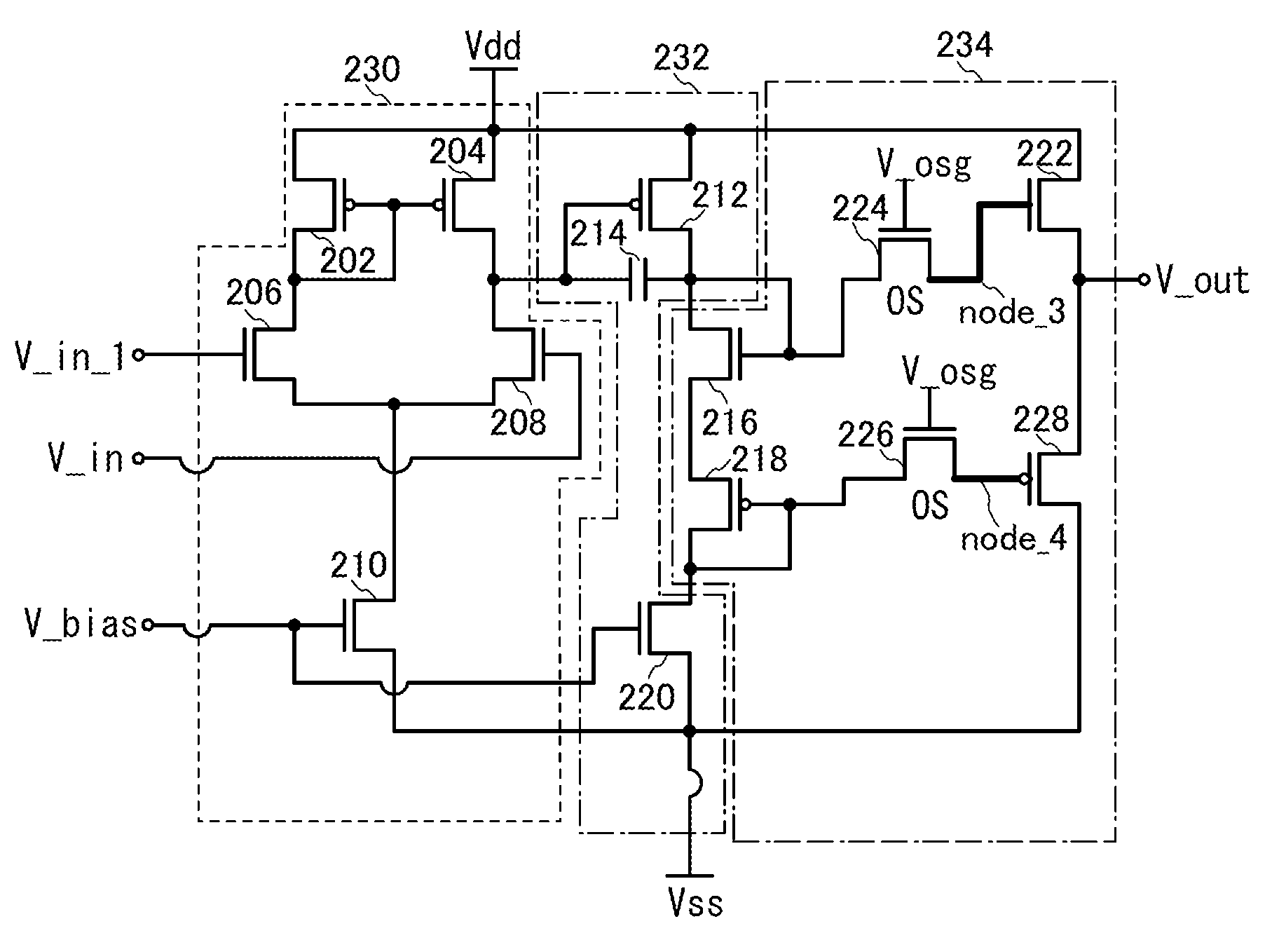
[0088]For example, FIG. 3 illustrates a voltage follower 200 which is a configuration example of a voltage follower including three stages: a differential amplifier 230, a gain stage 232, and an output stage 234. Note that the voltage follower 200 is a variation example of the voltage follower 100; thus, the reference numerals of the voltage follower 100 are used as appropriate in FIG. 3.
[0089]A voltage follower 200 in FIG. 3 includes first to thirteen...
embodiment 3
[0137]In this embodiment, a method for manufacturing a transistor included in the semiconductor device described in any of the above embodiments will be described.
[0138]In the voltage follower described in any of the above embodiments, the p-channel and n-channel transistors are formed by a general method using a substrate including a semiconductor material. Note that in this embodiment, one of the p-channel and n-channel transistors is illustrated over a semiconductor substrate for simplicity of the drawings.
[0139]A transistor with extremely low off-state current is formed in the following manner: p-channel and n-channel transistors are formed over a substrate including a semiconductor material and then a transistor including an oxide semiconductor is formed over the p-channel and n-channel transistors. In addition, a semiconductor substrate 700 over which p-channel and n-channel transistors are provided is used as a formation substrate and a transistor including an oxide semicondu...
PUM
 Abstract
Description
Claims
Application Information