Solvent vapor bonding and surface treatment methods

a technology of surface treatment and solvent, applied in the field of surface treatment and bonding of microstructured substrates, can solve the problems of poor dimensional accuracy, high cost, unsuitable for rapid prototyping,

Inactive Publication Date: 2012-11-15
UNIV OF SOUTHAMPTON
View PDF3 Cites 25 Cited by
  • Summary
  • Abstract
  • Description
  • Claims
  • Application Information

AI Technical Summary

Benefits of technology

[0047]For example, the surface bearing the microfluidic channel features or other microstructured features can have a surface roughness in the regio

Problems solved by technology

Injection molding requires a precision metal master, which is expensive and unsuited to rapid-prototyping24.
Wax printing produces a poor surface finish and low aspect ratio devices28.
Novel materials such as polystyrene (Shrinkydinks) have also been used to create microfluidic chips34 although with poor dimensional accuracy caused by shrinking of the substrates.
Therefore, many of the current rapid prototyping techniques show promise for low-cost realization of microfluidic designs, but they often compromise optical quality, are not cost-effective or retain some dependence on cle

Method used


Image

  • Solvent vapor bonding and surface treatment methods
  • Solvent vapor bonding and surface treatment methods
  • Solvent vapor bonding and surface treatment methods

Examples


examples

[0172]The present invention will now be described with reference to the following non-limiting examples.

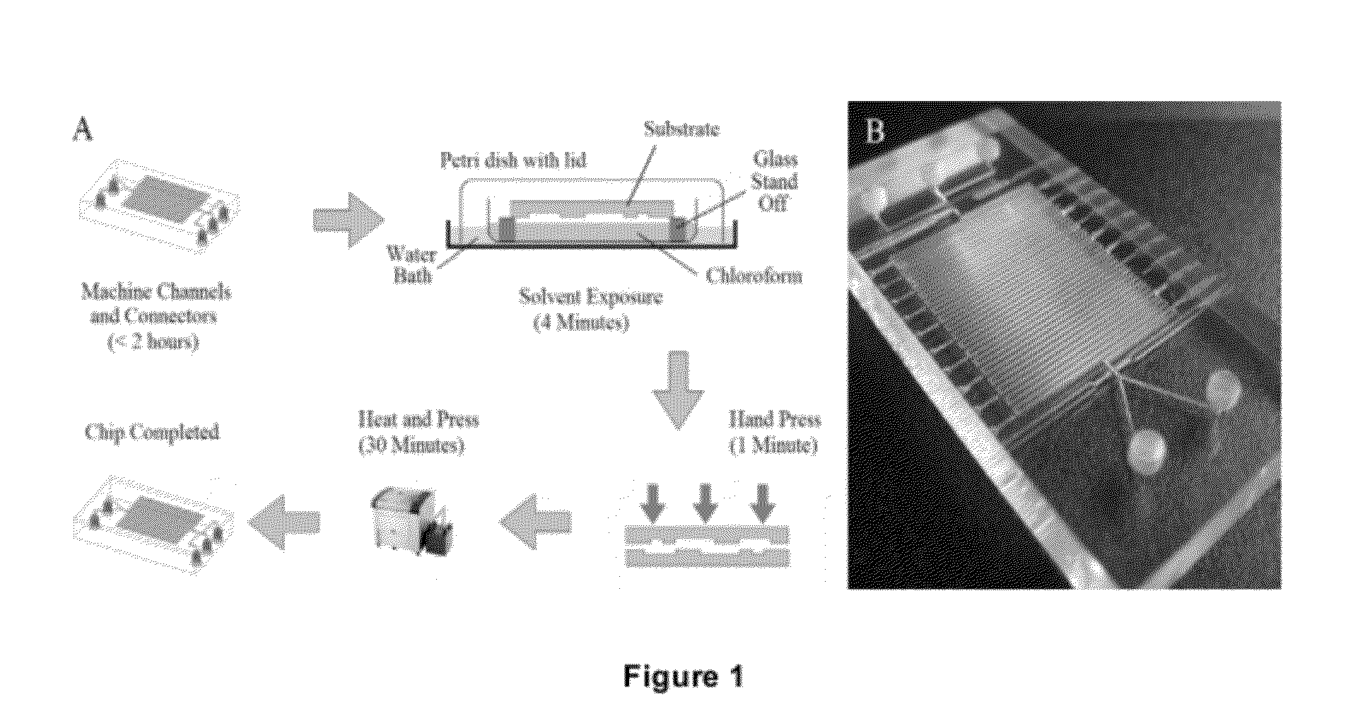
[0173]1.1 General Bonding of Two poly(methyl methacrylate) (PMMA) Polymer Substrates (Schematically shown in FIG. 1)

[0174]Fabrication

[0175]PMMA sheets (thicknesses from 1.5 mm to 8 mm) were obtained from (Röhm, Darmstadt, Germany). Channels were fabricated and ports / threads for MINSTAC microfluidic connectors (The Lee Company, Connecticut, USA) were machined into the plastics prior to bonding. The design was created using Circuitcam software (LPKF laser and electronics AG, Garbsen, Germany), software which calculates tool paths. This data was then imported into BoardMaster software (LPKF) which controls an automated LPKF Protomat S100 micro-mill (LPKF Laser and Electronics AG, Garbsen, Germany) which was used to mill channels and cut out the substrates.

[0176]Solvent Bonding

[0177]For solvent bonding, the two halves were aligned using a custom made jig which had a series of pins set...


PUM

PropertyMeasurementUnit
Timeaaaaaaaaaa
Timeaaaaaaaaaa
Surface roughnessaaaaaaaaaa

Abstract

The present invention relates to a method of producing a microstructured device, as well as a method of processing a microstructured substrate to heal surface defects therein, a method of bonding substrates and healing surface defects in a substrate, and microstructured devices produced by these methods.

Description

FIELD OF THE INVENTION[0001]This invention relates to methods of surface treatment and bonding of microstructured substrates using solvent vapour.BACKGROUND TO THE INVENTION[0002]Microfluidic devices are useful tools for the analysis of a variety of fluids, including chemical and biological fluids. These devices are primarily composed of microfluidic channels—for example input and output channels, plus structured areas for sample diagnosis. For effective processing of the fluid by the device, the fluid controllably passes through these channels.[0003]Various types of microfluidic devices are known. The channel cross-section dimensions in a microfluidic device can vary widely, but may be anything from the millimeter scale to the nanometer scale. Reference to microfluidics in this document is not restricted to micrometer scale devices, but includes both larger (millimeter) and smaller (nanometer) scale devices as is usual in the art.[0004]A basic form of a microfluidic device is based...

Claims


Application Information

Patent Timeline
IPC IPC(8): B32B3/00B32B37/14B29C65/00B32B37/02
CPCB29C65/4895Y10T428/24355B29C66/54B29C66/71B29C66/73161B29C66/7392B29C66/73921B29L2031/756B29C66/949B32B37/0076B32B38/162B81C3/001C09J5/00B32B2309/04B29C65/8253B01L3/502792B01L3/502761B01L3/502707B81C2203/032B81B2201/058B81B2201/0214B29C65/8223B29C65/8215B29K2023/06B29K2023/12B29K2023/18B29K2027/06B29K2033/20B29K2027/18B29K2029/14B29K2033/12B29K2025/06B29K2023/083B29K2033/04B29K2025/08B29K2023/38B29K2995/0072B29C66/73117B33Y80/00B29K2031/04
Inventor OGILVIE, IAIN RODNEY GEORGEFLOQUET, CEDRIC FLORIAN AYMERICMORGAN, HYWELSIEBEN, VINCENT JOSEPHMOWLEM, MATTHEW CHARLES
Owner UNIV OF SOUTHAMPTON
Why Eureka
Try Eureka