Signal processing circuit

Active Publication Date: 2012-11-22
SEMICON ENERGY LAB CO LTD
View PDF8 Cites 31 Cited by
  • Summary
  • Abstract
  • Description
  • Claims
  • Application Information

AI Technical Summary

Benefits of technology

[0033]In the signal processing circuit having the above structure, without moving a data signal between modules, input and standby of a data signal before and after supply of the power supply voltage is stopped can be performed. Therefore,

Problems solved by technology

In the memory element formed using a ferroelectric, a ferroelectric material is fatigued by repetition of data writing, which causes a problem such as a writing error.
As a result, the number of rewriting times is limited in the memory element formed using a ferroelectric.
Therefore, there are problems in that the memory circuit i

Method used


Image

  • Signal processing circuit
  • Signal processing circuit
  • Signal processing circuit

Examples


embodiment 1

[0084]In this embodiment, an example of a signal processing circuit and an example of a method of driving the signal processing circuit will be described with reference to FIGS. 1A and 1B, FIG. 2, FIG. 3, FIG. 4, FIGS. 5A and 5B, FIGS. 6A and 6B, and FIGS. 7A and 7B.

[0085]Note that the signal processing circuit includes large scale integrated circuits (LSIs) such as a CPU, a microprocessor, an image processing circuit, a digital signal processor (DSP), and a field programmable gate array (FPGA) in its category.

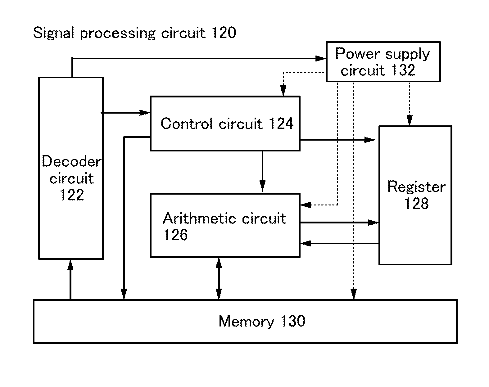
[0086]An example of a structure of a signal processing circuit will be described with reference to FIG. 1A. FIG. 1A is a block diagram schematically illustrating a structure of a signal processing circuit.

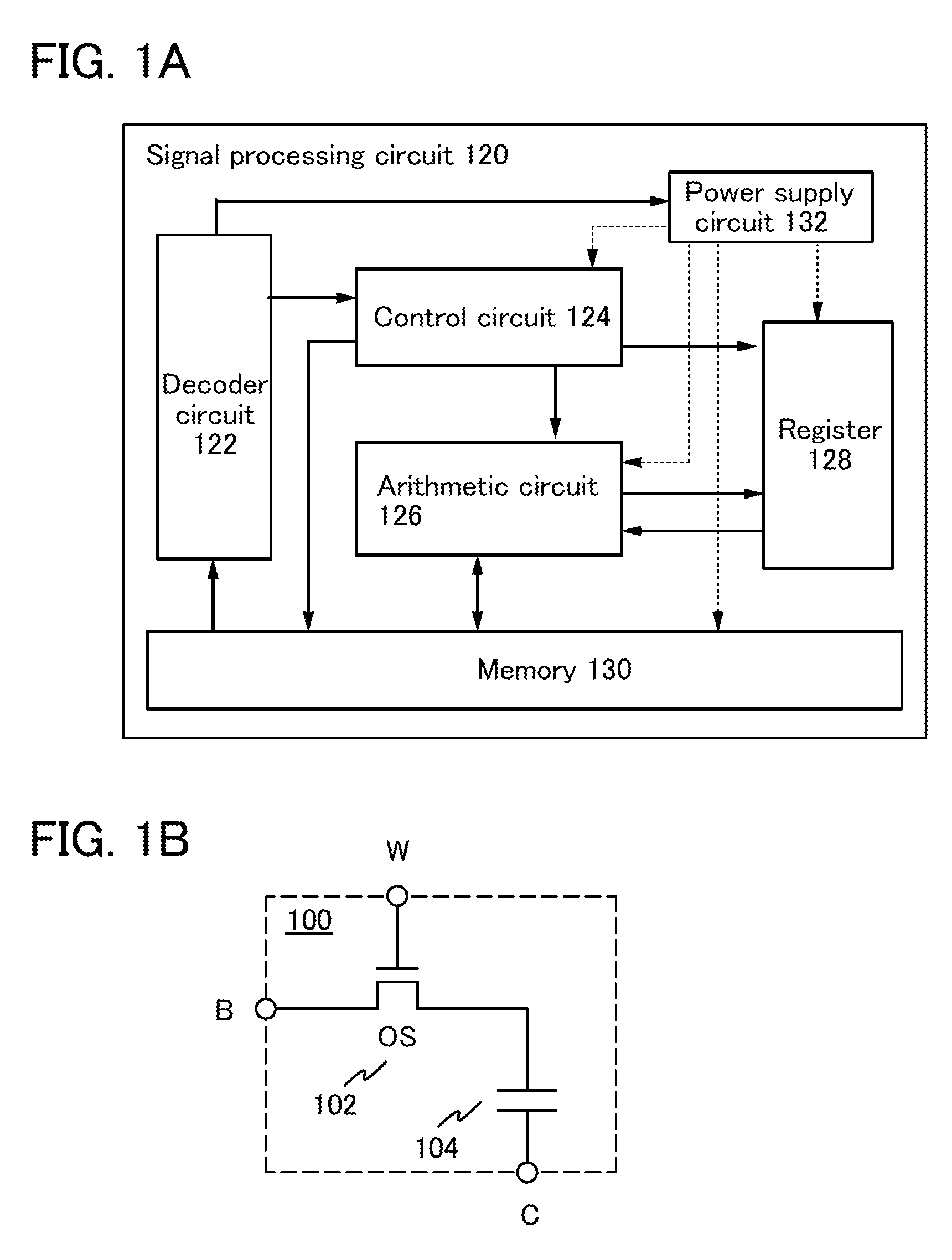
[0087]A signal processing circuit 120 includes a decoder circuit 122, a control circuit 124, an arithmetic circuit 126 (also referred to as an arithmetic logic unit (ALU)), a register 128, a memory 130, and a power supply circuit 132.

[0088]The decoder circuit 122 decodes a co...

embodiment 2

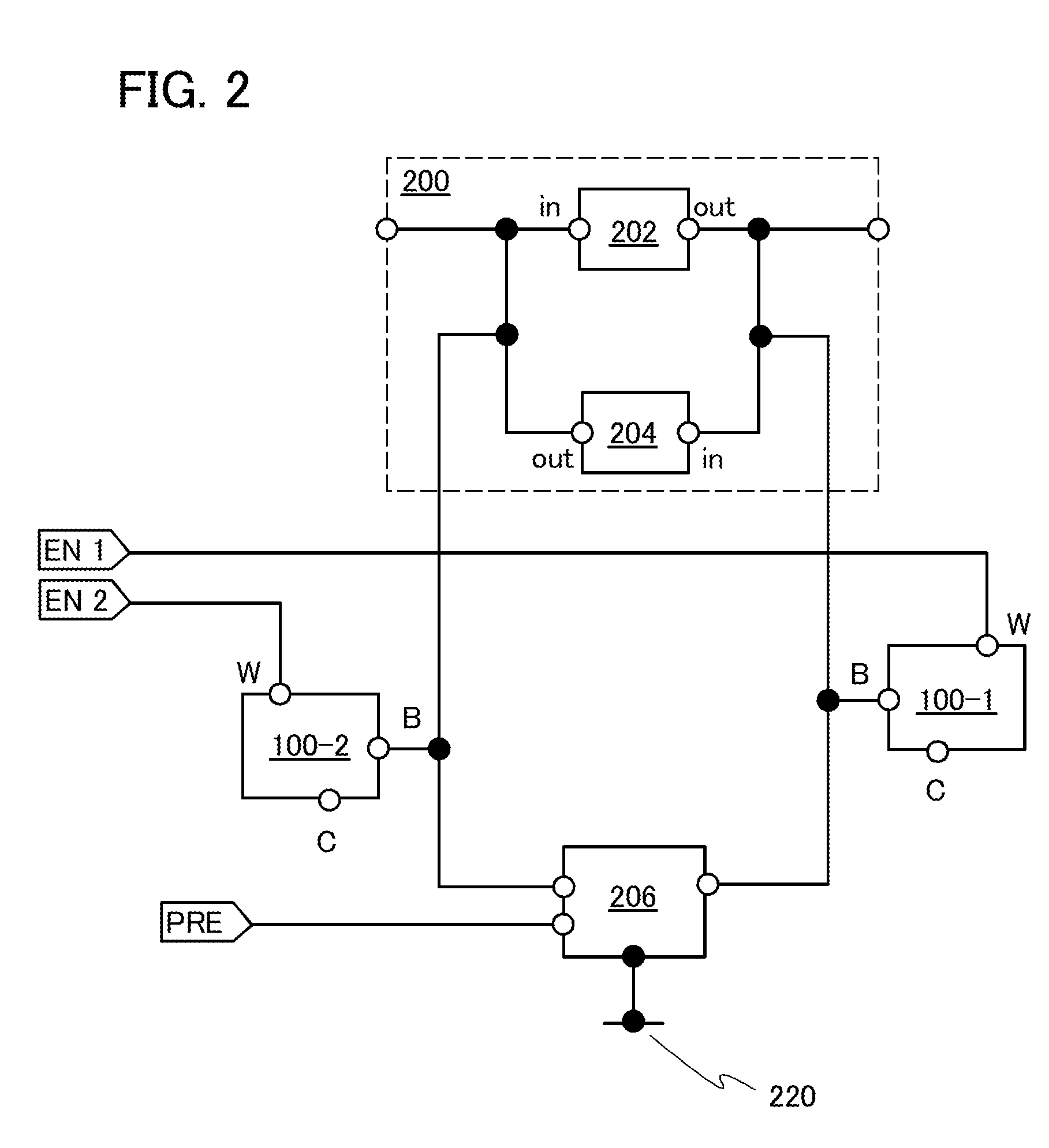
[0212]In Embodiment 1, an example of a structure applicable to the control circuit 124, the arithmetic circuit 126, and the register 128 which are included in the signal processing circuit is described with reference to FIG. 2 and the like.

[0213]In this embodiment, an example of a structure applicable to the control circuit 124, the arithmetic circuit 126, and the register 128, which is different from the above structure, will be described with reference to FIG. 8. Note that the control circuit 124, the arithmetic circuit 126, and the register 128 are also collectively referred to as a control portion. Here, at least one of the control circuit 124, the arithmetic circuit 126, and the register 128 includes a volatile memory circuit and plural pairs of non-volatile memory circuits corresponding to the volatile memory circuit.

[0214]FIG. 8 illustrates an example in which one volatile memory circuit 200 that can store a 1-bit data signal is provided with a plurality of non-volatile memor...

embodiment 3

[0273]In Embodiments 1 and 2, examples of a structure applicable to the control circuit 124, the arithmetic circuit 126, and the register 128 which are included in the signal processing circuit are described with reference to FIG. 2, FIG. 8, and the like.

[0274]In this embodiment, a structure in which a volatile memory circuit is also used as a latch circuit of a flip-flop circuit will be described with reference to FIG. 9.

[0275]FIG. 9 illustrates an inverter circuit 902 and an inverter circuit 904 which form a volatile memory circuit. These inverter circuits correspond to the arithmetic circuit 202 and the arithmetic circuit 204 described in Embodiment 1 with reference to FIG. 2.

[0276]A DRAM circuit can be formed using the volatile memory circuit (the inverter circuit 902 and the inverter circuit 904) and the pair of non-volatile memory circuits (the non-volatile memory circuit 100-1 and the non-volatile memory circuit 100-2). Note that the number of pairs of non-volatile memory cir...


PUM


Abstract

A signal processing circuit includes a memory and a control portion configured to control the memory. The control portion includes a volatile memory circuit including data latch terminals, a first non-volatile memory circuit electrically connected to one of the data latch terminals, a second non-volatile memory circuit electrically connected to the other of the data latch terminals, and a precharge circuit having a function of supplying a potential that is a half of a high power supply potential to the one and the other of the data latch terminals. Each of the first non-volatile memory circuit and the second non-volatile memory circuit includes a transistor having a channel formation region including an oxide semiconductor and a capacitor connected to a node that is brought into a floating state by turning off the transistor.

Description

BACKGROUND OF THE INVENTION[0001]1. Field of the Invention[0002]The present invention relates to a signal processing circuit including a memory circuit in which a stored logic state is not lost even after power is turned off, and to an electronic device using the signal processing circuit. Further, the present invention relates to a method of driving a signal processing circuit including a memory circuit in which a stored logic state is not lost even after power is turned off.[0003]2. Description of the Related Art[0004]Signal processing circuits such as central processing units (CPUs) vary in structure depending on the intended use. A signal processing circuit generally has a main memory for storing data or a program and other memory circuits such as a register and a cache memory.[0005]A register has a function of temporarily holding data in order to carry out arithmetic processing or hold a program execution state, for example. In addition, a cache memory is located between an ari...

Claims


Application Information

Patent Timeline
IPC IPC(8): G11C11/24G11C7/10
CPCH01L27/1052H01L27/108G11C11/413H01L27/1203H01L27/1225H01L27/115H10B99/00H10B12/00H10B69/00G11C5/06G11C5/14G11C7/10G11C7/22G11C14/0009
Inventor OHMARU, TAKUROKOBAYASHI, HIDETOMO
Owner SEMICON ENERGY LAB CO LTD
Why Eureka
Try Eureka