Housing for electronic device and method for manufacturing the same

a technology for electronic devices and housings, applied in the field of housings, can solve the problems of easy scratching and cracking, operator's inability to form patterns, text, or pictures on the substrate via pvd process,

Inactive Publication Date: 2012-11-22
HONG FU JIN PRECISION IND (SHENZHEN) CO LTD +1
View PDF4 Cites 18 Cited by
  • Summary
  • Abstract
  • Description
  • Claims
  • Application Information

AI Technical Summary

Benefits of technology

[0006]Another method to produce such decorative plastic housings is physical vapor deposition (PVD) process PVD is a process of depositing thin films by the condensation of a vaporized form of the material onto various surfaces. In this way, a metallic film can be deposited on a surface of a substrate, and the substrate can render great metallic luster. Nevertheless, the operator cannot form patterns text, or pictures on the substrate via PVD process. Furthermore, after depositing a metallic film on the substrate, a coating of protecting layer is deposited on the plastic substrate and the thickness of the housing increases. The coating area is large the protection layer and is easily to scratch and crack. Therefore, there is room for improvement in the art.
[0005]In-Mold Labeling (IML) process is a typical method to produce such decorative plastic housing. The process is carried out by molding a plastic substrate to combine with a plastic film in a mold. Prior to the substrate being molded, a predetermined pattern, text, or picture is printed on the film. The molded substrate is then combined with the patterned film. The pattern may not be abraded or eroded because it is located between the film and the substrate. However, a coating with metallic luster cannot be formed on the substrate in this manner.

Problems solved by technology

However, a coating with metallic luster cannot be formed on the substrate in this manner.
Nevertheless, the operator cannot form patterns text, or pictures on the substrate via PVD process.
The coating area is large the protection layer and is easily to scratch and crack.

Method used


Image

  • Housing for electronic device and method for manufacturing the same
  • Housing for electronic device and method for manufacturing the same
  • Housing for electronic device and method for manufacturing the same

Examples


first embodiment

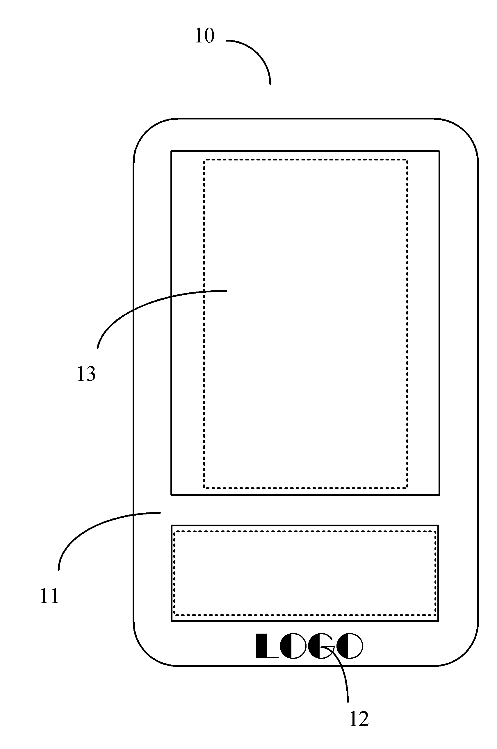
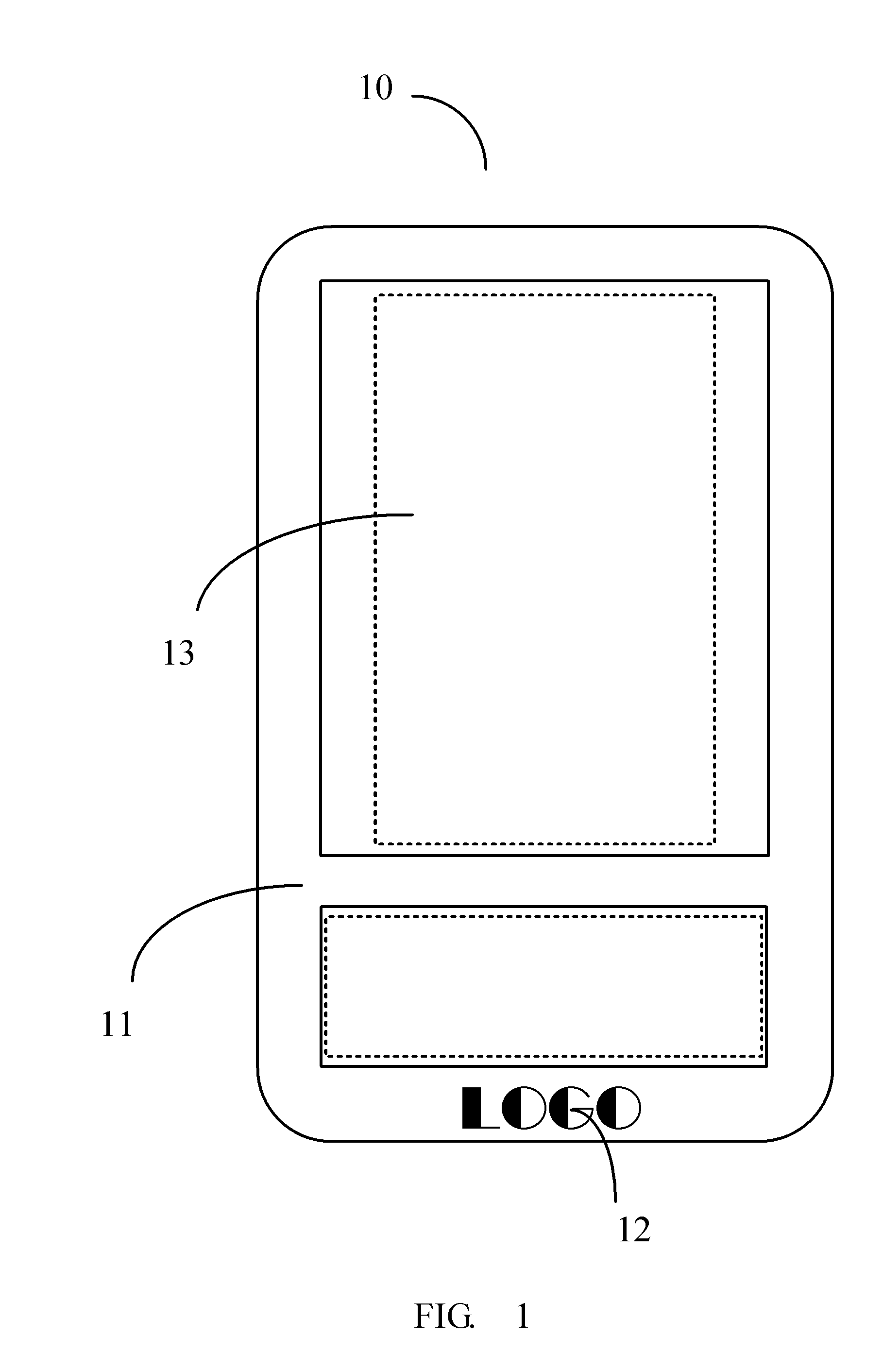
[0019]Referring to FIG. 3, a flowchart of a process of manufacturing the housing 11 is illustrated.

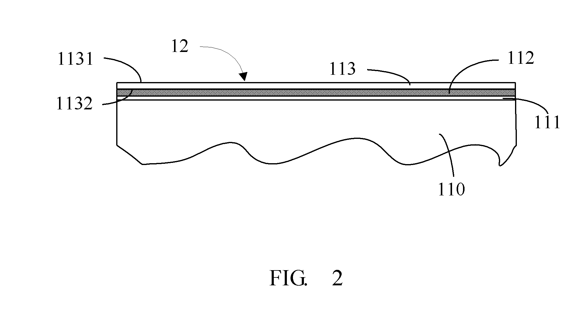
[0020]In step S11, providing a transparent film including a first surface and an opposing second surface. The transparent film may be made of a material selected from the group consisting of polyisoprene (PI), polycarbonate (PC), or polyethylene terephthalate (PET), and any suitable combination thereof. The thickness of the transparent film is about 0.1 to about 0.5 mm.

[0021]In step S12, forming a metallic film on the first surface of the transparent film. The metallic film can be deposited on the first surface of the transparent film using physical vapor deposition (PVD) process.

[0022]In step S13, applying adhesive material on the metallic film to form an adhesive layer 111 on the metallic film, the second surface is free of the adhesive material thereon.

[0023]In step S14, placing the treated transparent film in a mold, and the second surface of the transparent film attached to the i...

second embodiment

[0030]Referring to FIG. 5, a flowchart of a process of manufacturing the housing 11 is illustrated.

[0031]In step S21, providing a transparent film including a first surface and an opposing second surface. The transparent film may be made of a material selected from the group consisting of polyisoprene (PI), polycarbonate (PC), or polyethylene terephthalate (PET), and any suitable combination thereof. The thickness of the transparent film is about 0.1 to about 0.5 mm.

[0032]In step S22, applying a pattern layer on the first surface of the transparent film. A predetermined decorative pattern, text or image can be printed on the predetermined regions of the first surface of the transparent film to form the pattern layer 124.

[0033]In step S23, applying a metallic film layer on the first surface of the transparent film. The metallic film can be deposited on the first surface of the transparent film to cover the pattern layer with physical vapor deposition (PVD) process.

[0034]In step S24,...


PUM

PropertyMeasurementUnit
thicknessaaaaaaaaaa
thicknessaaaaaaaaaa
transparentaaaaaaaaaa

Abstract

A method of manufacturing a housing includes steps of providing a transparent film including a first surface and an opposing second surface. Forming a patterned layer on the first surface of the transparent film, forming a metallic film layer on the first surface of the transparent film to cover the patterned layer, applying an adhesive material on the metallic film. Then placing the transparent film in the mold, the second surface of the transparent film attached to the inner molding surface of the mold. And at last injecting plastic material into the mold to form a plastic base adhered with the transparent film. The housing can have both predetermined patterns and metallic luster.

Description

BACKGROUND[0001]1. Technical Field[0002]The present disclosure relates to housings, particularly to a housing for electronic devices and a method of manufacturing the housing.[0003]2. Description of Related Art[0004]The external appearance of the housing of the portable electronic devices (such as mobile telephones and electronic notebooks) has become a key factor for attracting consumers.[0005]In-Mold Labeling (IML) process is a typical method to produce such decorative plastic housing. The process is carried out by molding a plastic substrate to combine with a plastic film in a mold. Prior to the substrate being molded, a predetermined pattern, text, or picture is printed on the film. The molded substrate is then combined with the patterned film. The pattern may not be abraded or eroded because it is located between the film and the substrate. However, a coating with metallic luster cannot be formed on the substrate in this manner.[0006]Another method to produce such decorative pl...

Claims


Application Information

Patent Timeline
Patent Type & Authority Applications(United States)
IPC IPC(8): B32B15/00B32B38/00
CPCY10T428/1352H05K5/0243
Inventor TANG, CHAOQIN, SHENG-CHANGLUO, ZHONG-JIEDAI, JIAN-HUICHEN, YU-TAOJAN, TE-SHENGYEN, CHUN-CHE
Owner HONG FU JIN PRECISION IND (SHENZHEN) CO LTD
Why Eureka
Try Eureka