[0016]The present technique provides
level shifting circuitry comprising two level shifters, one for triggering an output in response to the rising edge transition and the other for triggering an output in response to the falling edge transition. Each level shifter responds to the input signal by generating an intermediate signal having a primary transition and a secondary transition. In the first level shifter, the primary transition is generated in response to a falling edge transition and the secondary transition is generated in response to a rising edge transition, and in the second level shifter, the primary transition is generated in response to the rising edge transition and the secondary transition generated in response to the falling edge transition. The first level shifter is faster than the second level shifter when responding to a falling edge transition, and the second level shifter is faster than the first level shifter when responding to a rising edge transition.
[0017]The output signal is switched between the output high voltage level and the output low voltage level in response to the primary transitions of the first and second intermediate signals. The secondary transitions of the first and second intermediate signals do not have a significant
impact on the output signal. Each level shifter can be designed to generate the primary transition relatively quickly without needing to consider the response speed of the secondary transition. The
level shifting circuitry can therefore respond relatively quickly to both edges of the input signal, allowing the level shifting circuitry to operate at higher frequencies.
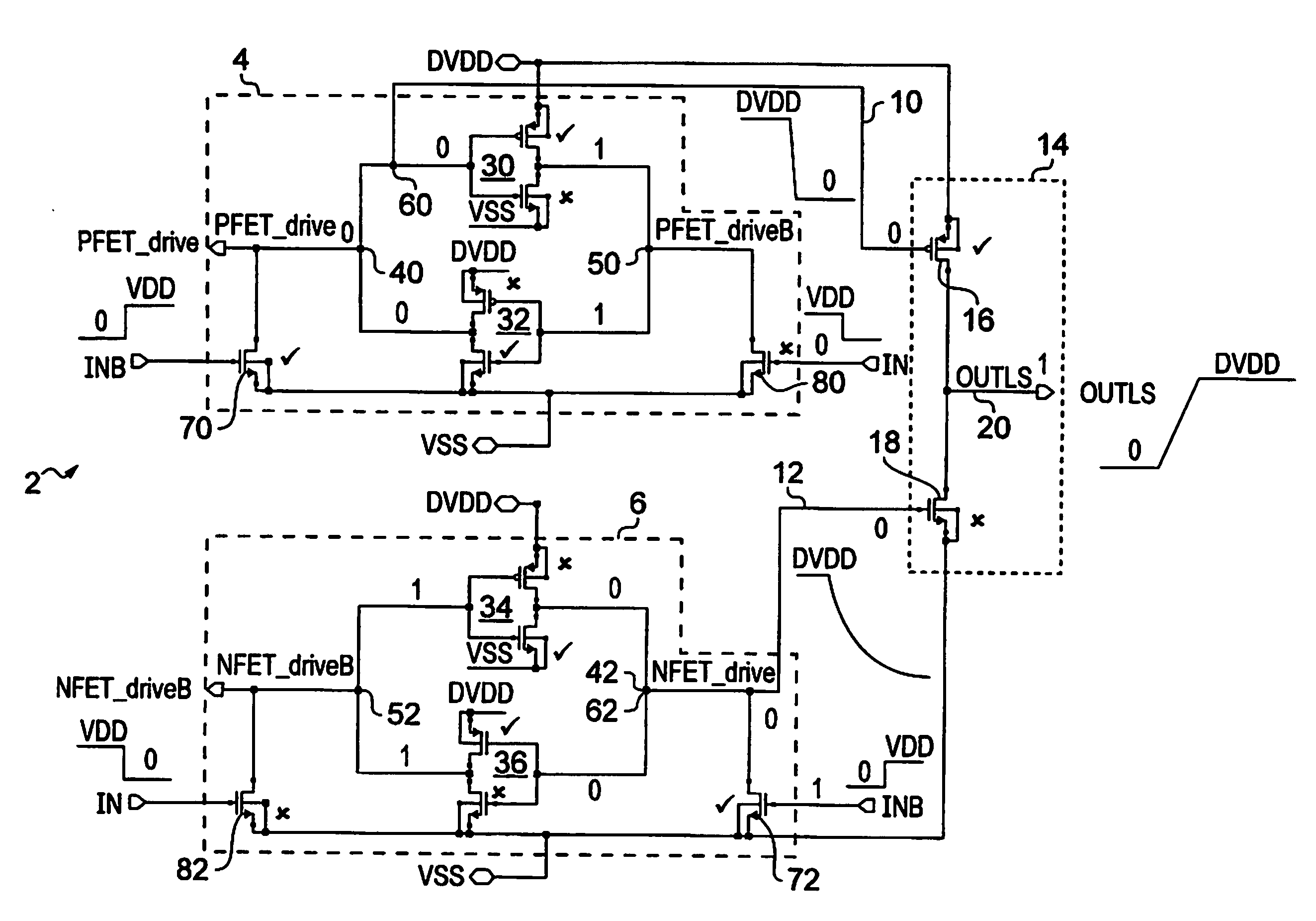
[0021]In one embodiment, the first level shifter may comprise a first
feedback loop which retains signal values in one of a first state and a second state in dependence on the input signal, and the second level shifter may comprise a second
feedback loop which retains signal values in one of the first and second states in dependence on the input signal. In the feedback loops, the first or second intermediate signal may be obtained from an intermediate output point of the
feedback loop. Hence, the respective feedback loops are placed in the first state or second state in dependence on the current value of the input signal, and the first and second intermediate signals take on values corresponding to the current state of the feedback loops. This arrangement provides a compact circuit
layout.
[0026]In one particularly advantageous embodiment, the level shifting circuitry may comprise an additional pullup
transistor which selectively assists the pullup
transistor in pulling the output signal to the output high voltage level and an additional pulldown
transistor which selectively assists a pulldown transistor in pulling the output signal to the output low voltage level. When one of the pullup and pulldown transistors is being switched on in response to the primary transition of one intermediate signal, the other transistor is being switched off in response to the secondary transition of the other intermediate signal. Since the secondary transition is slower than the primary transition, the other transistor is switched off slowly and so there is a period during which the other transistor competes against the transistor being switched on, slowing the transition of the output signal. To speed up the transition of the output signal, the additional pullup transistor and additional pulldown transistor can be used to boost the pull of the transistor being switched on, so as to pull the output signal to its new value more quickly. This further increases the maximum operational frequency of the level shifting circuitry.
[0027]Additional pullup control circuitry may be provided to control the operation of the additional pullup transistor, and additional pulldown control circuitry may be provided to control the operation of the additional pulldown transistor. In advance of the primary transition of the first intermediate signal and the secondary transition of the second intermediate signal, the additional pullup control circuitry may couple the gate of the additional pullup transistor to one of the first intermediate signal and the second intermediate signal, and the additional pulldown control circuitry may decouple the gate of the additional pulldown transistor from the other of the first and second intermediate signals. This means that, when the primary transition of the one intermediate signal and the secondary transition of the other signal intermediate signal occur, then both the pullup transistor and the additional pullup transistor will become active and will compete with the pulldown transistor. The additional pulldown transistor will be inactive. Hence the combined drive strength of the pullup transistors is stronger than the drive strength of the pulldown transistor, and so the output signal is quickly pulled to the output high voltage level. Similarly, in response to the other transition, the additional pullup and pulldown control circuitry may configure the additional pullup and pulldown transistors so that the pulldown transistor and additional pulldown transistor compete against the pullup transistor to rapidly pull the output signal down to the output low voltage level. Hence, faster output signal transitions are achieved.
[0031]The additional pullup transistor may have a greater drive strength than the pullup transistor and the additional pulldown transistor may have a greater drive strength than the pulldown transistor. The greater the drive strength of the additional pullup transistor and the additional pulldown transistor, the greater the boost provided by the additional transistors in pulling the output
signal level to the output high voltage level or the output low voltage level, and hence the greater the frequency at which the level shifting circuitry can operate.

