Nonvolatile Full Adder Circuit

a full adder circuit, nonvolatile technology, applied in the direction of computation using denominational number representation, pulse technique, instruments, etc., can solve the problems of power off, loss of logic state, data loss,

Inactive Publication Date: 2012-12-06
SHUKH ALEXANDER MIKHAILOVICH +1
View PDF2 Cites 6 Cited by
  • Summary
  • Abstract
  • Description
  • Claims
  • Application Information

AI Technical Summary

Benefits of technology

[0014]Disclosed herein is a nonvolatile full adder circuit comprising: a full adder electrical circuitry comprising first input terminal for receiving first binary input signals, a second input terminal for receiving second binary input signals, a third input terminal for receiving binary carry-in signals, a first output terminal for providing a sum output signal, and a second output terminal for providing a carry-out signal; a high voltage source electrically coupled to a first source terminal of the full adder electrical circuitry; a low voltage source electrically coupled to a second source terminal of the full adder electrical circuitry; a first nonvolatile memory element co

Problems solved by technology

They can lose their logic states when the power is

Method used


Image

  • Nonvolatile Full Adder Circuit
  • Nonvolatile Full Adder Circuit
  • Nonvolatile Full Adder Circuit

Examples


second embodiment

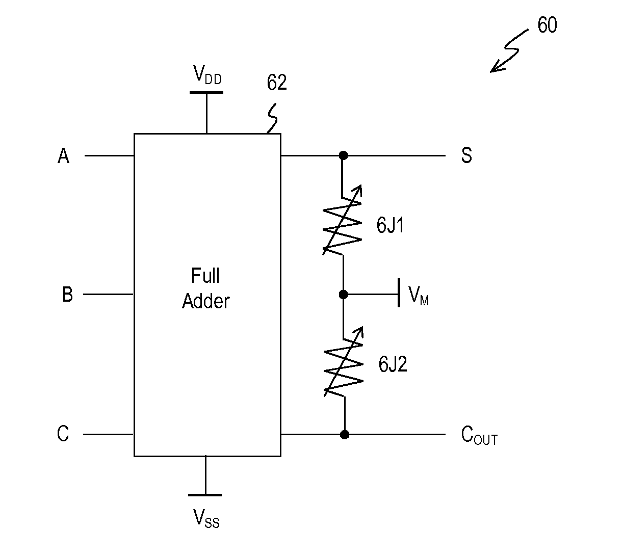
[0034]FIGS. 4A and 4B show transistor-level circuit diagrams of nonvolatile logic modules 40-1 and 40-2 implementing SUM (FIG. 4A) and CARRY (FIG. 4B) functions, respectively according to the disclosure. The modules 40-1 and 40-2 represent a nonvolatile complementary pass-transition logic (CPL) full adder. The sum logic module 40-1 (FIG. 4A) can comprise four logic blocks 41-44. The logic block 41 is a matrix block comprising eight nMOS transistors 4N1-4N8 with twelve inputs for A, A*, B, B*, C, and C* signals. The nonvolatile logic block 42 represents a pull-up block comprising two pMOS transistors 4P1 and 4P2, and two MR elements 4J1 and 4J2. The memory element 4J1 can be connected to drain terminals (or to a common drain terminal) of the transistors 4P1, 4N5, and 4N6 at its first end and to the memory voltage source VM at its second end. Respectively, the MR element 4J2 can be connected to the drain terminals (or to a common drain terminal) of the transistor 4P2, 4N7, and 4N8 at ...

third embodiment

[0039]FIGS. 5A and 5B show a transistor-level and gate-level circuit diagrams of a nonvolatile one-bit full adder 50 constructed according to the present disclosure. The diagrams represent the nonvolatile transmission-gates full adder 50.

[0040]The transistor-level nonvolatile full adder 50 is shown in FIG. 5A. It can include four inverters 501-504, six transmission gates 51-56, two pMOS transistors 5P1, 5P2 and two nMOS transistors 5N1, 5N2 connected in series, and two nonvolatile MR elements 5J1 and 5J2. The transmission gate 51 can comprise an pMOS transistor 5P3 and an nMOS transistor 5N3 connected in parallel to each other. The transmission gates 52-56 can have similar design. The MR element 5J1 can be electrically coupled to the output terminal of the inverter 503 at its first end and to the memory voltage source VM at its second end to provide a nonvolatile storage of the logic value S. Respectively, the MR element 5J2 can be electrically coupled to the output terminal of the ...


PUM


Abstract

A nonvolatile full adder circuit comprising a full adder electrical circuitry comprising three input terminals for receiving two input and carry-in signals, a sum output terminal, and an carry-out output terminal; first and second nonvolatile memory elements electrically coupled to the first and second output terminal, respectively at their first ends and to an intermediate voltage source at their second ends. The nonvolatile memory elements comprise two stable logic states. A logic state each of the of the nonvolatile memory elements is controlled by a bidirectional electrical current running between its first and second ends. The full adder circuitry is electrically coupled to a high voltage source at its first source terminal and to a low voltage source at its second source terminal, wherein an electrical potential of the intermediate voltage source is lower than that of the high voltage source but higher than that of the low voltage source.

Description

CROSS-REFERENCE TO RELATED APPLICATIONS[0001]This application claims the benefit of provisional patent application No. 61 / 493,407 filed on Jun. 3, 2011 by the present inventors.FEDERALLY SPONSORED RESEARCH[0002]Not ApplicableSEQUENCE LISTING OR PROGRAM[0003]Not ApplicableRELEVANT PRIOR ART[0004]U.S. Pat. No. 8,135,768, Mar. 13, 2012—Stewart[0005]U.S. Patent Application Publication No. US 2012 / 0105105, May 3, 2012—Shukh[0006]Matsunaga S. et al., Fabrication of Nonvolatile Full Adder Based on Logic-in-Memory Architecture Using Magnetic Tunnel Junctions, Applied Physics Express, vol. 1, 091301, 2008.[0007]Kang S.-M. et al., CMOS Digital Integrated Circuits: Analysis and Design, 3rd edition, McGraw-Hill Companies, Inc., 2003.BACKGROUND[0008]A full adder is a fundamental logic circuit of numerous logic devices such as microcontrollers, processors, field programmable gate arrays (FPGAs) and many others. In general, a full adder represents an electronic circuit that has several inputs and ...

Claims


Application Information

Patent Timeline
IPC IPC(8): H03K19/21
CPCH03K19/16H03K19/215
Inventor SHUKH, ALEXANDER MIKHAILOVICHAGAN, TOM A.
Owner SHUKH ALEXANDER MIKHAILOVICH
Why Eureka
Try Eureka