Semiconductor structure and method for manufacturing the same

a semiconductor and structure technology, applied in the field of semiconductor structure, can solve the problems of limiting the room for shortening the gate height, affecting the overall speed of the logic architecture operated integrated circuit, and affecting the current drive capability and power consumption, so as to achieve reduce the effect of gate height and effective shortened gate heigh

Inactive Publication Date: 2012-12-13
EARTH WALL PRODS LLC +2
View PDF25 Cites 9 Cited by
  • Summary
  • Abstract
  • Description
  • Claims
  • Application Information

AI Technical Summary

Benefits of technology

[0008]The present invention aims to provide a semiconductor structure and its manufacturing method, which is favorable for effectively reducing the gate height, thereby reducing capacitance between the metal gate and contact regions, and lowering the requirement for process preciseness and difficulty to etch through holes.
[0017]As compared to the prior art, the semiconductor structure and its manufacturing method provided by the present invention exhibit the following advantages:
[0018]At formation of a gate stack, a CMP stop layer is applied such that the poly silicon layer may be removed at the time of performing planarization process, which accordingly is stopped at the CMP stop layer. Usually, the planarization process is stopped at a poly silicon layer, whereas the present invention proposes to introduce a CMP stop layer, whose hardness is greater than that of a poly silicon layer, such that the poly silicon layer may be removed at the time of performing the planarization process and thus the gate height shall be effectively shortened. In the conventional process, it is impossible to fabricate a very thin gate stack mainly because when source and drain are implanted with ions, the gate would be easily penetrated through, if the gate has been made very thin. However, after formation of the source and drain, a planarization process is performed till the poly silicon layer is removed, such that the CMP stop layer added by the present invention is exposed, thus the gate height is effectively shortened. Meanwhile, owing to the decrease in the gate height, the capacitance between the gate and the contact regions would be reduced. Additionally, because the difference of heights between the gate and source / drain becomes smaller, the distance to be etched become shorter at the time of etching through holes. Therefore, compared to the traditional process for etching through holes, it becomes easier to control the etching distance and accuracy, which therefore optimizes the process of etching through holes.

Problems solved by technology

Thus, requirements of process control during manufacturing a semiconductor device become increasingly stringent.
The capacitance between the gate and source / drain extensions not only affects the current drive capability and power consumption, but also affects significantly the overall speed of the integrated circuit operated in logic architectures.
The traditional CMOS process limits the room for shortening the gate height.
Therefore, along with decrease in the gate height, the lower layer of gate oxide is more probably polluted by gate dopants.
However, because of reduction of the thermal budget, the dopants in other electrodes may not be sufficiently activated, which might consequently curb the drive current.
However, the lowered implantation energy for the self-aligned source / drain and Halo would cause a high source / drain parasitic capacitance, which makes the Halo inside the channel not doped sufficiently, reduces the drive current and even impairs the short channel roll-off characteristics.
Conversely, when traditional MOS process of Raised Source / Drain (RSD) is applied to reduce the relative gate height, it would be affected by the unnecessarily Temporary Enhanced Diffusion (TED).
Boron), which is harmful to devices with short channels, for example, increasing the roll-off rate of threshold voltages.

Method used


Image

  • Semiconductor structure and method for manufacturing the same
  • Semiconductor structure and method for manufacturing the same
  • Semiconductor structure and method for manufacturing the same

Examples


Embodiment Construction

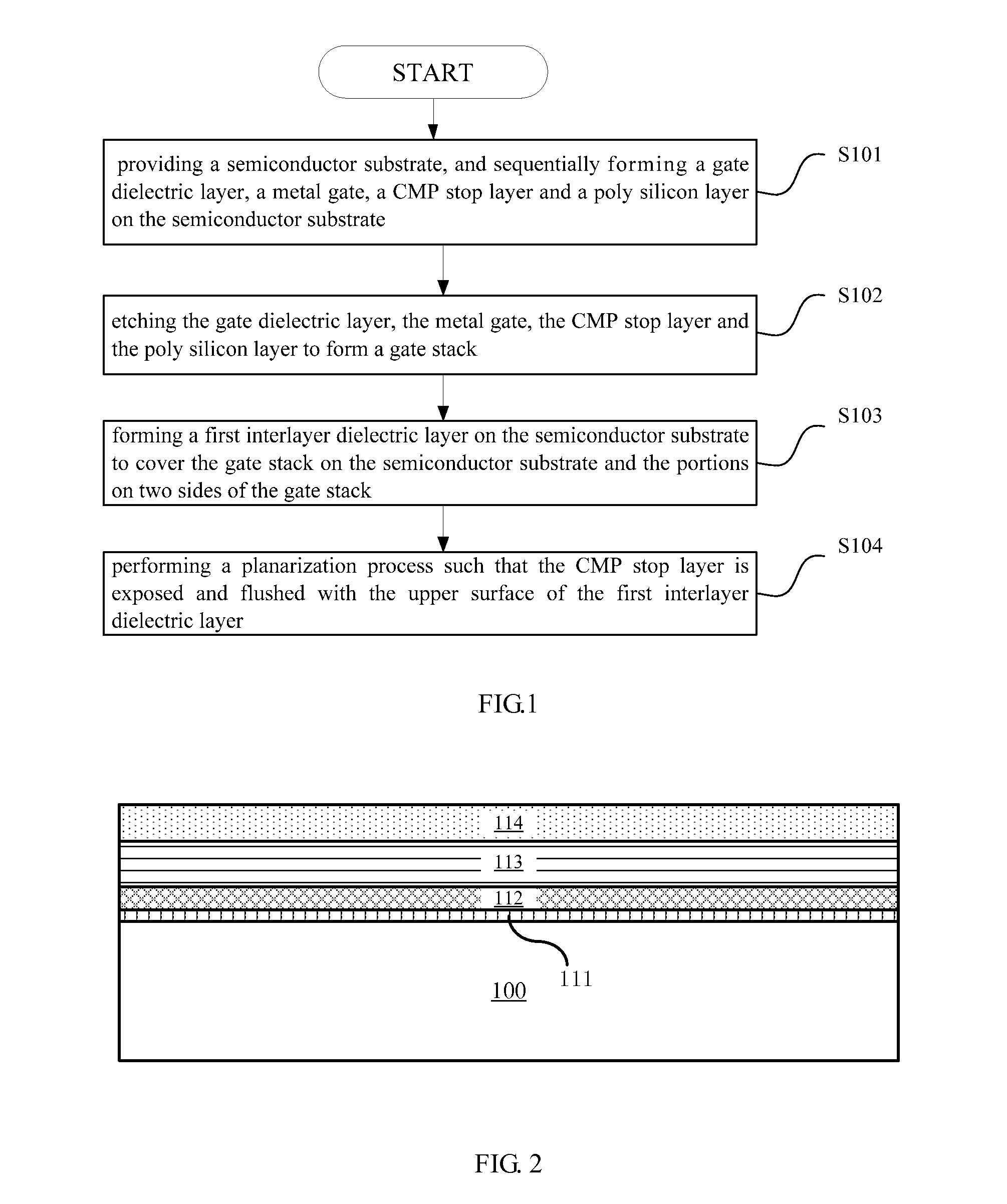
[0023]Objectives, technical solutions, and advantages of the present invention are made more evident according to the following detailed description of exemplary embodiments in conjunction with the accompanying drawings.

[0024]Embodiments of the present invention are described here below, wherein the examples of the embodiments are illustrated in the drawings, in which same or similar reference signs throughout denote same or similar elements or elements have same or similar functions. It should be appreciated that the embodiments described below in conjunction with the drawings are illustrative and are provided for explaining the present invention only. Thus, they shall not be interpreted as a limit to the present invention.

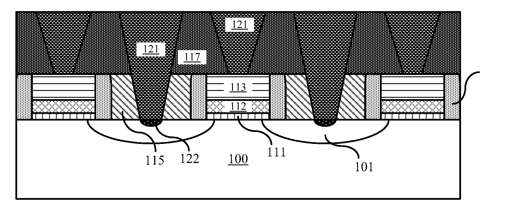
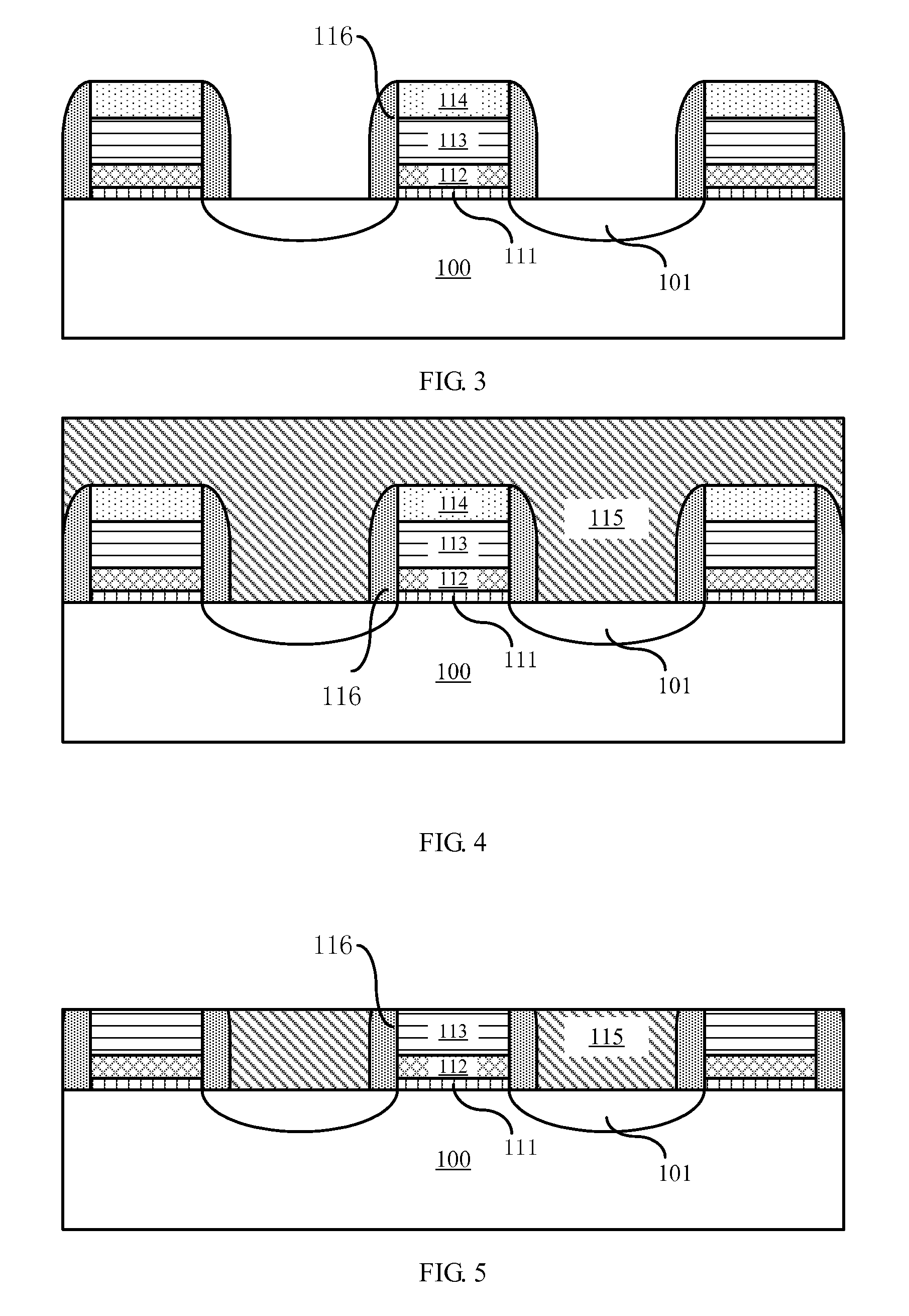
[0025]Various embodiments or examples are provided here below to implement different structures of the present invention. To simplify the disclosure of the present invention, description of the components and arrangements of specific examples is given below. Of c...


PUM

PropertyMeasurementUnit
total thicknessaaaaaaaaaa
thicknessaaaaaaaaaa
thicknessaaaaaaaaaa

Abstract

The present invention provides a semiconductor structure and a method for manufacturing the same. The method comprises the following steps: providing a semiconductor substrate, forming sequentially a gate dielectric layer, a metal gate, a CMP stop layer, and a poly silicon layer on the semiconductor substrate; etching the gate dielectric layer, the metal gate, the CMP stop layer and the poly silicon layer to form a gate stack; forming a first interlayer dielectric layer on the semiconductor substrate to cover the gate stack on the semiconductor substrate and the portions on both sides of the gate stack; performing a planarization process, such that the CMP stop layer is exposed and flushed with the upper surface of the first interlayer dielectric layer. Accordingly, the present invention further provides a semiconductor structure. Through adding the CMP stop layer, the present invention is able to effectively shorten the height of a metal gate, thus effectively reduces the capacitance between the metal gate and contact regions, and therefore optimizes the subsequent process for etching through holes.

Description

[0001]The present application claims priority benefit of Chinese Patent Application No. 201110154452.1 titled “Semiconductor Structure and Method for Manufacturing the Same” filed on 9 Jun. 2011, which is herein incorporated by reference in its entirety.FIELD OF THE INVENTION[0002]The present invention relates to semiconductor manufacturing, and specifically relates to a semiconductor structure and its manufacturing method.BACKGROUND OF THE INVENTION[0003]As the semiconductor industry develops, integrated circuits with better performance and more powerful functions require greater component density. Moreover, the size of and the space between the components become further scaled down (has already reached 45 nm or less at present time). Thus, requirements of process control during manufacturing a semiconductor device become increasingly stringent.[0004]The height of a gate stack affects the parasitic capacitance between the gate and source / drain (S / D) contact structures and their ele...

Claims


Application Information

Patent Timeline
Patent Type & Authority Applications(United States)
IPC IPC(8): H01L29/78H01L21/336
CPCH01L29/78H01L21/28518H01L21/76816H01L21/76814H01L29/66545
Inventor YIN, HAIZHOUZHU, HUILONGLUO, ZHIJIONG
Owner EARTH WALL PRODS LLC
Why Eureka
Try Eureka