

Semiconductor memory device
a memory device and semiconductor technology, applied in the direction of digital storage, solid-state devices, instruments, etc., can solve the problems of difficult line disposal and difficult manufacturing process, and achieve the effect of increasing the integration degree and reducing the number of lines for each memory block
- Summary
- Abstract
- Description
- Claims
- Application Information
AI Technical Summary
Benefits of technology
Problems solved by technology
Method used
Image

Examples
Embodiment Construction
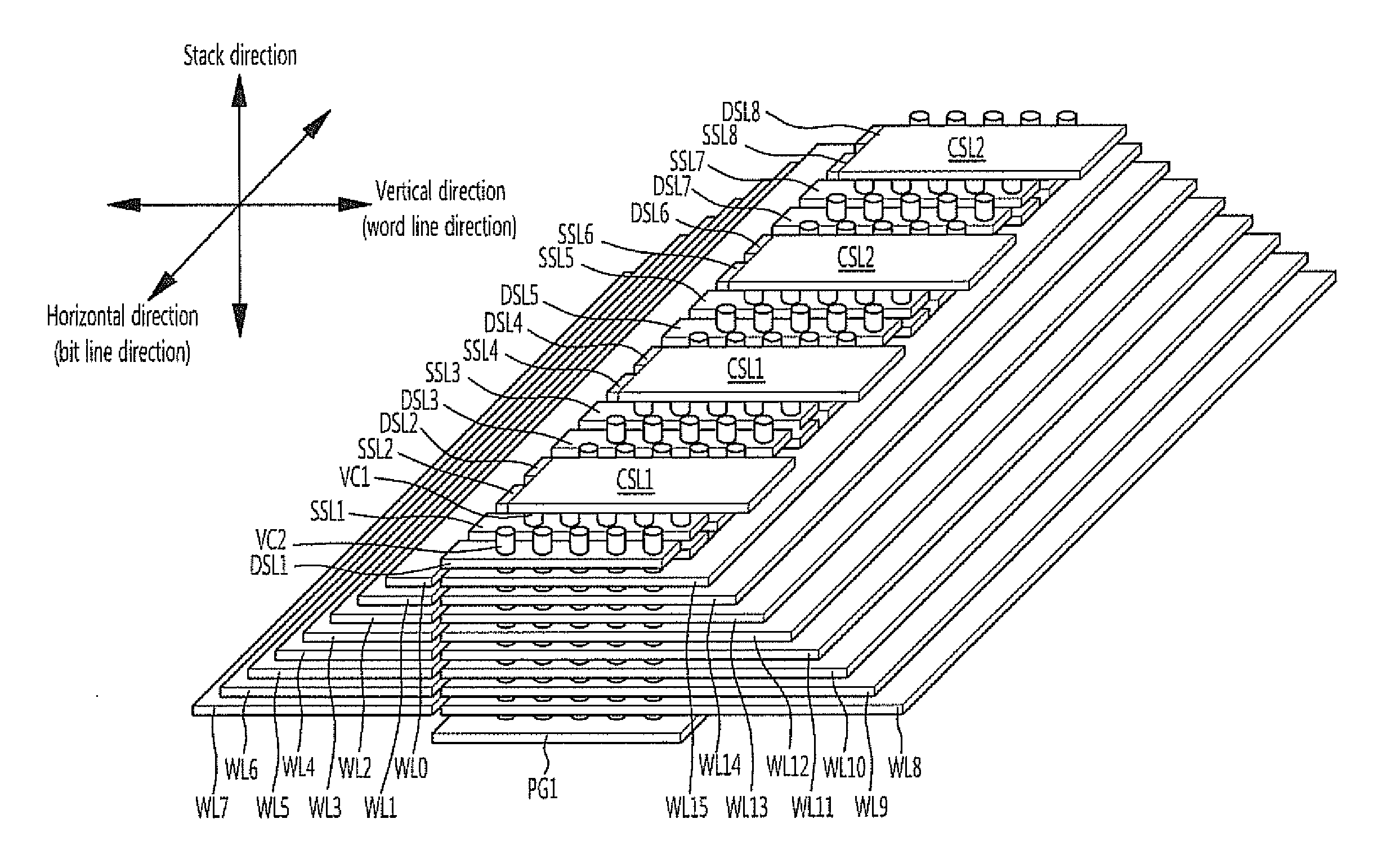
[0022]Hereinafter, some exemplary embodiments of the present disclosure will be described in detail with reference to accompanying drawings. The figures are provided to allow those having ordinary skill in the art to understand the scope of the embodiments of the disclosure.
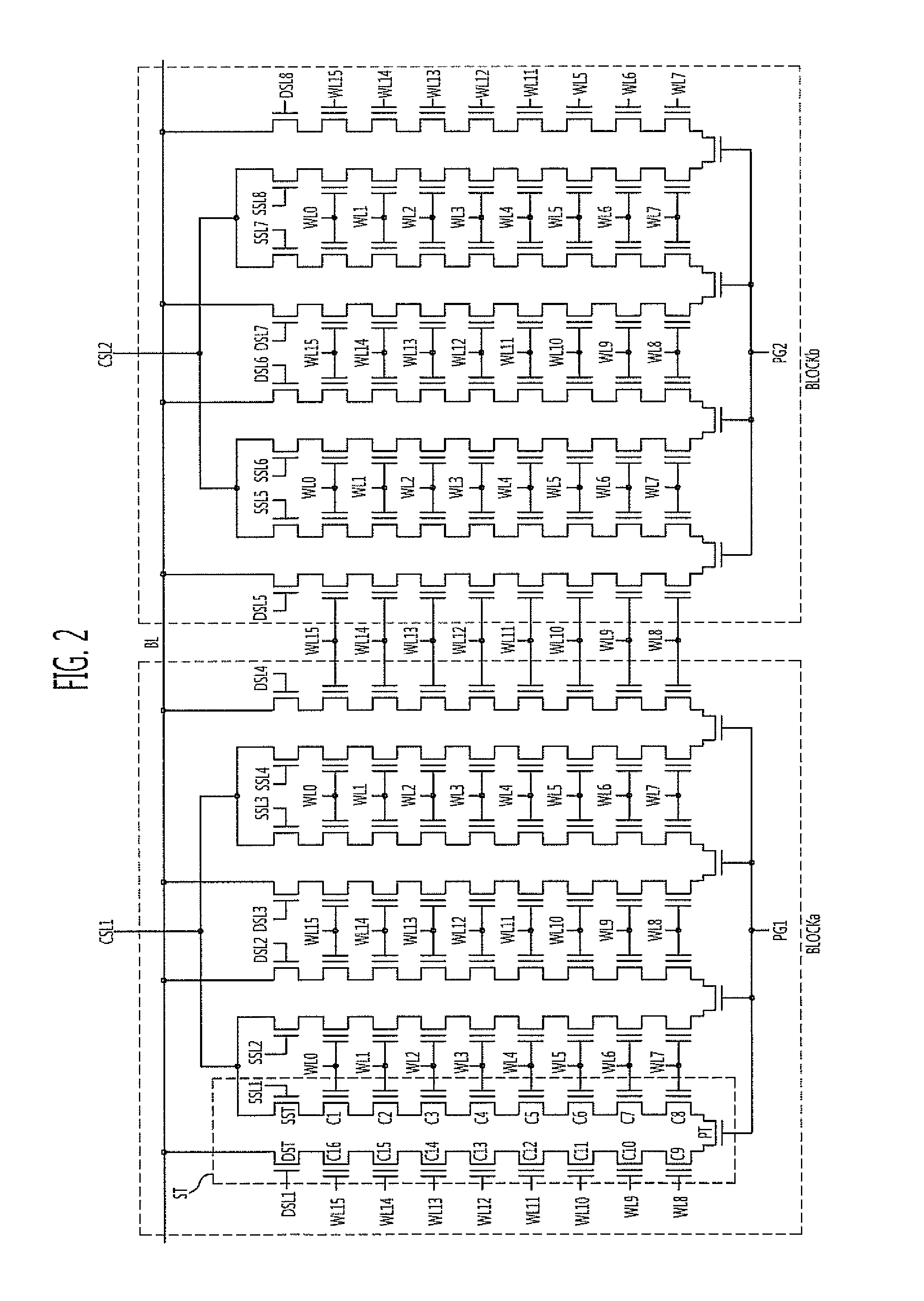
[0023]FIG. 2 is a circuit diagram illustrating a memory block having a P-BiCS structure according to an exemplary embodiment of this disclosure.
[0024]Referring to FIG. 2, each of memory blocks BLOCKa and BLOCKb includes a plurality of memory strings ST. Each of the memory strings ST includes a drain select transistor DST having a drain coupled to a bit line BL (only one bit line is shown, for illustration purposes), a source select transistor SST having a source coupled to a common source line CSL1, and a plurality of memory cells C1 to C16 coupled in series between the select transistors (that is, the drain select transistor DST and the source select transistor SST). Here, while the number of memory cells may be...
PUM
 Abstract
Description
Claims
Application Information