Display panel and gate driving circuit and driving method for gate driving circuit

Active Publication Date: 2012-12-20
AU OPTRONICS CORP
3 Cites 21 Cited by

AI-Extracted Technical Summary

Problems solved by technology

However, the backward-extended wire for delivering the charging gate driving pulse G(n) from the charging gate driving unit Ch[n] to the charging gate driving unit Ch[n−2] is arranged crossing multiple stages of charging gate driving unit and sharing gate driving unit, which ...

Method used

[0031]In comparing the charging gate driving unit string 110 of FIG. 3A according to the disclosure with that of FIG. 1A, each of the charging gate driving units in the charging gate driving unit string 110 such as Ch[3] uses the sharing gate driving pulse S(3) outputted from the sharing gate driving unit SR[3] in the sharing gate diving unit string 130 neighboring with the charging gate driving unit Ch[3] to enable the pull-down circuit 17 of the charging gate driving unit Ch[3], rather than uses the charging gate driving pulse G(5) outputted from the second succeeding-stage charging gate driving unit Ch[5] as a pull-down enabling pulse to enable the pull-down circuit of the charging gate driving unit Ch[3] as illustrated in FIG. 1A. Therefor...

Benefits of technology

[0008]A display panel in accordance with another embodiment includes multiple data lines, multiple gate lines disposed crossing over the data lines, multiple sharing control lines disposed next to the respective gate lines, multiple pixels, a first gate driving unit string and a second gate driving unit string. Each pixel is electrically coupled to one of the data lines, one of the gate lines and one of the sharing control lines. The multiple gate lines are configured for controlling corresponding pixels whether to receive data from corresponding data lines. The multiple sharing control lines are configured for controlling the corresponding pixels whether to share charges in the corresponding pixels respectively. The first gate driving unit string includes multiple cascade-connected fir...

Abstract

An exemplary gate driving circuit is adapted for driving a display panel including multiple pixels and includes a first gate driving unit string and a second gate driving unit string. The first gate driving unit string includes multiple cascade-connected first gate driving units and receives a start pulse. The first gate driving units are for generating output pulses to drive the pixels. The second gate driving unit string includes multiple cascade-connected second gate driving units and receives the start pulse. The second gate driving units are for generating output pulses to drive the pixels. The output pulse generated from one of the second gate driving units is provided to one of first gate driving units to determine whether to disable the output pulse of the first gate driving unit which receives the output pulse generated from the second gate driving units.

Application Domain

Cathode-ray tube indicatorsDigital storage +1

Technology Topic

AND gateDriving circuit

Image

  • Display panel and gate driving circuit and driving method for gate driving circuit
  • Display panel and gate driving circuit and driving method for gate driving circuit
  • Display panel and gate driving circuit and driving method for gate driving circuit

Examples

  • Experimental program(1)

Example

[0023]The disclosure will now be described more specifically with reference to the following embodiments. It is to be noted that the following descriptions of embodiments are presented herein for purpose of illustration and description only. It is not intended to be exhaustive or to be limited to the precise form disclosed.
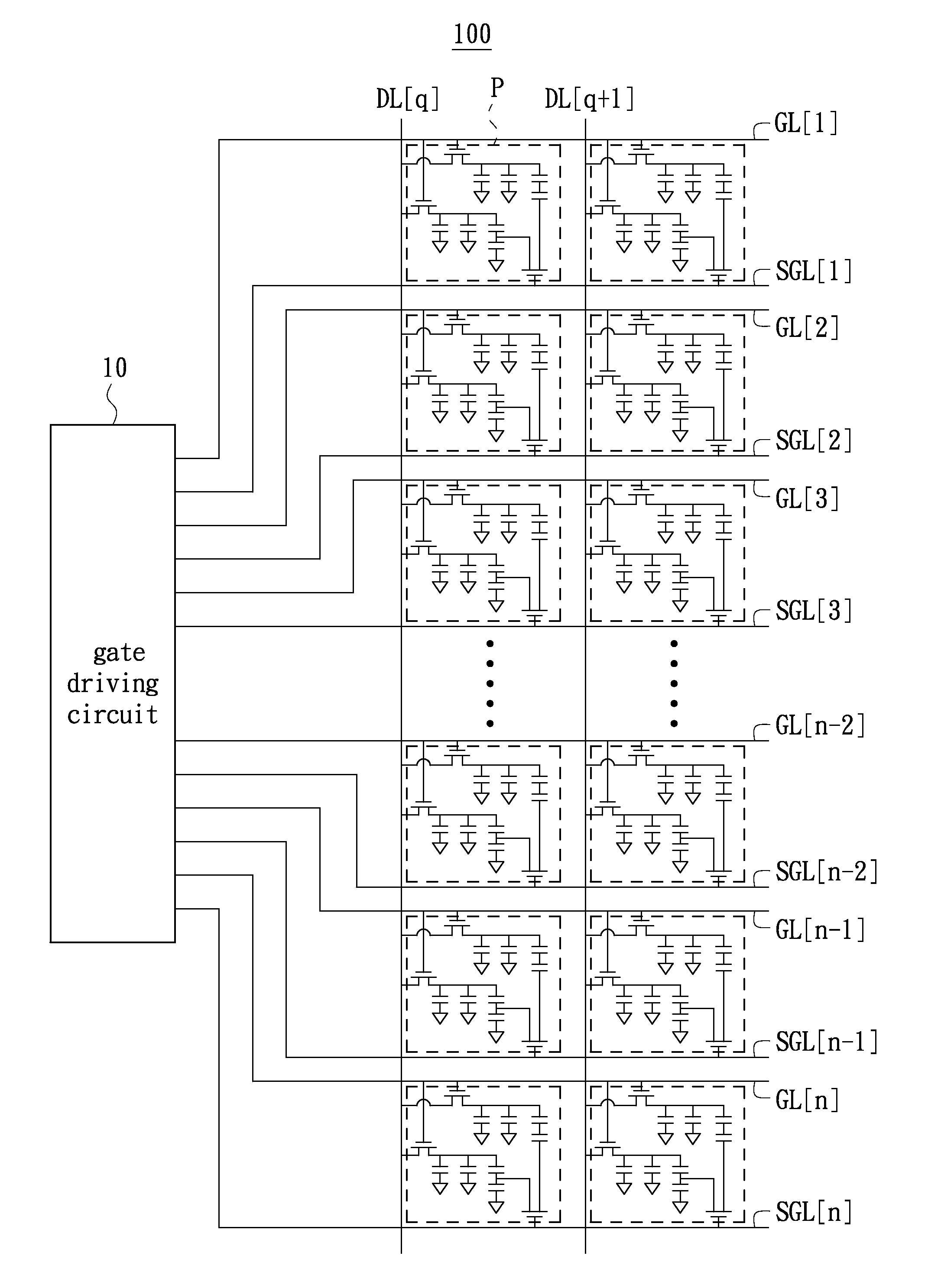
[0024]Referring to FIG. 2, FIG. 2 is a schematic partial structure view of a display panel according to an embodiment. In the illustrated embodiment, the display panel 100 may be a liquid crystal display panel or other kind of active-driven display panel, and includes a gate driving circuit 10, multiple pixels P, multiple data lines such as DL[q] and DL[q+1], multiple gate lines GL[1]-GL[n] and multiple sharing control lines SGL[1]-SGL[n]. Each of the data lines DL[q] and DL[q+1] is used to provide display data to corresponding pixels P. Each of the gate lines GL[1]-GL[n] is electrically coupled to the gate driving circuit 10 and disposed crossing over the data lines DL[q] and DL[q+1]. Each of the sharing control lines SGL[1]-SGL[n] is electrically coupled to the gate driving circuit 10 and disposed in next to the respective gate lines GL[1]-GL[n]. Each of the pixels P is electrically coupled to one of the data lines DL[q] and DL[q+1], one of the gate lines GL[1]-GL[n] and one of the sharing control lines SGL[1]-SGL[n] to determine whether to receive the display data from the corresponding data line by the corresponding gate line and determine whether to internally share charges in the pixel by the corresponding sharing control line. Each of the pixels P includes multiple e.g., two sub-pixels mutually sharing charges. The circuit configuration of the two sub-pixels of each pixel P can refer to the description associated with FIG. 1B and thus will not be repeated herein.
[0025]Referring to FIGS. 3A through 3D, FIG. 3A is a schematic configuration of the gate driving circuit 10 of the display panel 100 in FIG. 2 according to an embodiment, FIG. 3B is schematic waveforms of driving pulses outputted from the gate driving circuit 10 in a single frame F(m), FIG. 3C is a schematic detailed circuit diagram of a single charging gate driving unit in FIG. 3A, and FIG. 3D is schematic waveforms of multiple signals relevant to the gate driving circuit of FIG. 3C.
[0026]As shown in FIG. 3A, the gate driving circuit 10 includes a charging gate driving unit string 110 (namely, a first gate driving unit string) and a sharing gate driving unit string 130 (namely, a second gate driving unit string). The charging gate driving unit string 110 includes charging gate driving units Ch[1]-Ch[n] and dummy charging gate driving units Ch[DM1]-Ch[DM2] all connected in cascade. The charging gate driving unit string 110 receives a start pulse ST and generates output pulses stage by stage so that the charging gate driving units Ch[1]-Ch[n] sequentially output charging gate driving pulses G(1)-G(n) to control whether the corresponding pixels P receive the display data from the corresponding data lines. Moreover, the charging gate driving unit string 110 receives high frequency clock signals e.g., HC1, HC2, HC3, HC4, HC5, HC6 and low frequency clock signals e.g., LC1, LC2. Each of the charging gate driving units Ch[1]-Ch[n] and dummy charging gate driving units Ch[DM1]-Ch[DM2] receives two of the high frequency clock signals e.g., HC1, HC3 (or HC2, HC4; or HC3, HC5; or HC4, HC6; or HC1, HC5; or HC2, HC6) and the low frequency clock signals LC1, LC2.
[0027]The sharing gate driving unit string 130 includes delay sharing gate driving units SR[DMA]-SR[DMB], sharing gate driving units SR[1]-SR[n] and dummy sharing gate driving units SR[DM1]-SR[DM4] all connected in cascade. When the sharing gate driving unit string 130 receives the start pulse ST, the start pulse ST is firstly transferred by the delay sharing gate driving units SR[DMA]-SR[DMB], and then generates output pulses transferred to the sharing gate driving units SR[1]-SR[n] stage by stage so that the sharing gate driving units SR[1]-SR[n] sequentially output sharing gate driving pulses S(1)-S(n) respectively to the sharing control lines SGL[1]-SGL[n] to control whether the corresponding pixels P internally share charges. Moreover, the sharing gate driving unit string 130 also receives the high frequency clock signals e.g., HC1, HC2, HC3, HC4, HC5, HC6 and the low frequency clock signals e.g., LC1, LC2. Each of the delay sharing gate driving units SR[DMA]-SR[DMB], sharing gate driving units SR[1]-SR[n] and dummy sharing gate driving units SR[DM1]-SR[DM4] receives two of the high frequency clock signals e.g., HC1, HC3 (or HC2, HC4; or HC3, HC5; or HC4, HC6; or HC1, HC5; or HC2, HC6) and the low frequency clock signals LC1, LC2.
[0028]With regard to one of the charging gate driving units e.g., Ch[n] and one of the sharing gate driving units e.g., SR[n] for driving a same pixel P, the sharing gate driving pulse S(n) outputted from the sharing gate driving unit SR[n] is provided to the charging gate driving unit Ch[n] to determine whether to disable the charging gate driving pulse G(n) outputted from the charging gate driving unit Ch[n], that is, to determine whether to stop charging so as to carry out charge sharing. In this embodiment, the gate line and the sharing control line respectively controlled by the charging gate driving unit and the sharing gate driving unit for driving the same pixel P are disposed at two sides of the pixel P and neighboring with each other. It can be found from the waveform diagram of FIG. 3B, effective times of the charging gate driving pulse such as G(n) and the sharing gate driving pulse S(n) for driving the same pixel P are not overlapped with each other, while effective times of two neighboring charging gate driving pulses such as G(n−1) and G(n) are partly overlapped with each other, for example overlapped with 50%, and effective times of two neighboring sharing gate driving pulses such as S(n−1) and S(n) also are partly overlapped with each other. It is indicated that, the waveforms of each of the charging gate driving pulses G(1)-G(n) and each of the sharing gate driving pulses S(1)-S(n) in FIG. 3B are simulated waveforms obtained under the situation of the effect of internal circuits of the gate driving circuit 10 being in consideration, while ideally, each of the waveforms of the driving pulses G(1)-G(n) and S(1)-S(n) is an ideal square wave.
[0029]As shown in FIG. 3C, in the charging gate driving unit string 110, any one of the charging gate driving units Ch[1]-Ch[n] and dummy charging gate driving units Ch[DM1]-Ch[DM2] such as Ch[3] includes an enable control circuit 11, a pull-up circuit 13, a stabilizing circuit 15 and a pull-down circuit 17. The enable control circuit 11 is used to enable the pull-up circuit 13 and may include two transistors T11 and T12 connected in cascade. The gate of the transistor T12 receives an enabling voltage signal for example the voltage signal Q(1) at a node Q of the second preceding-stage charging gate driving unit Ch[1], the source/drain of the transistor T12 receives the high frequency clock signal HCl. The gate of the transistor T11 is electrically coupled to the drain/source of the transistor T12, the source/drain of the transistor T11 receives the charging gate driving pulse G(1) outputted from the second preceding-stage charging gate driving unit Ch[1], and the drain/source of the transistor T11 is electrically coupled the node Q of the charging gate driving unit Ch[3]. In short, the enable control circuit 11 receives the signals Q(1) and G(1) outputted from the second preceding-stage charging gate driving unit Ch[1] and the high frequency clock signal HCl to thereby generate an enabling voltage signal Q(3) at the node of the current-stage charging gate driving unit Ch[3]. It is understood that, the enable control circuit 11 may only include a single transistor instead. The pull-up circuit 13 is subjected to the control of the enabling voltage signal Q(3) to generate the charging gate driving pulse G(3) according to the high frequency clock signal HC3. The pull-up circuit 13 is for example includes a transistor T21. The gate of the transistor T21 is electrically coupled to the node Q of the charging gate driving unit Ch[3] and thereby the voltage signal Q(3) at the node Q of the charging gate driving unit Ch[3] determines whether to turn on the transistor T21, the source/drain of the transistor T21 receives another high frequency clock signal HC3, and the drain/source of the transistor T21 electrically coupled to the pull-down circuit serves as an output terminal of the charging gate driving pulse G(3). The stabilizing circuit 15 is used to stabilize the voltage at the node Q of the charging gate driving unit Ch[3] and the voltage of the drain/source of the transistor T21, and for example includes multiple transistors T32, T42, T51, T52, T53, T54, T33, T43, T61, T62, T63, T64 and a capacitor (not labeled). The transistors T32, T42, T51, T52, T53, T54 cooperatively constitute a first stabilizing unit, and the first stabilizing unit receives the low frequency clock signal LC1 and the signals Q(3), G(3) generated by the current-stage charging gate driving unit Ch[3]. The transistors T33, T43, T61, T62, T63, T64 cooperatively constitute a second stabilizing unit, and the second stabilizing unit receives the low frequency clock signal LC2 and the signals Q(3), G(3) generated by the current-stage charging gate driving unit Ch[3]. The pull-down circuit 17 for example includes transistors T31 and T41. The transistors T31, T41 both are subjected to the control of the sharing gate driving pulse S(3) outputted from the sharing gate driving unit SR[3] to pull the voltages respectively at the node Q and the drain/source of the transistor T21 down to a predetermined voltage level such as Vss in a particular time, that is, switching the charging gate driving pulse G(3) from an enabling state to a disabling state. Herein, it is indicated that, any one of the delay sharing gate driving units SR[DMA]-SR[DMB], sharing gate driving units SR[1]-SR[n] and dummy sharing gate driving units SR[DM1]-SR[DM4] may have the same detailed circuit configuration as that of the charging gate driving unit Ch[3] as illustrated in FIG. 3C, and thus will not be repeated, so that the signal at the node Q in SR[3] can be named as SQ(3).
[0030]As shown in FIG. 3D, schematic waveforms of the high frequency clock signals HC1-HC6, the low frequency clock signals LC1-LC2, the signals Q(3) and G(3) generated from the current-stage charging gate driving unit Ch[3], and the signals SQ(3) and S(3) outputted from the sharing gate driving unit SR[3] are illustrated. In this embodiment, the low frequency clock signals LC1, LC2 are mutually phase-inverted.
[0031]In comparing the charging gate driving unit string 110 of FIG. 3A according to the disclosure with that of FIG. 1A, each of the charging gate driving units in the charging gate driving unit string 110 such as Ch[3] uses the sharing gate driving pulse S(3) outputted from the sharing gate driving unit SR[3] in the sharing gate diving unit string 130 neighboring with the charging gate driving unit Ch[3] to enable the pull-down circuit 17 of the charging gate driving unit Ch[3], rather than uses the charging gate driving pulse G(5) outputted from the second succeeding-stage charging gate driving unit Ch[5] as a pull-down enabling pulse to enable the pull-down circuit of the charging gate driving unit Ch[3] as illustrated in FIG. 1A. Therefore, it is no longer necessary to arrange backward-extended wires crossing other stages of charging gate driving unit and sharing gate driving unit, the phenomenon of one backward-extended wire crossing multiple stages is avoided, the parasitic resistance and capacitance is decreased, the waveforms of charging gate driving pulses are improved and the whole power consumption is lowered and further the possibility of ESD damage is reduced. Moreover, the charging gate driving unit string 110 of the disclosure only needs two stages of dummy charging gate driving units, compared with the four stages of dummy charging gate driving units in FIG. 1A, the number of the dummy charging gate driving units is decreased and therefore the layout space is saved.
[0032]Referring to FIG. 3E, FIG. 3E is a schematic configuration of the gate driving circuit 10 from another viewpoint. For the convenience of drawing, the clock signals HC1˜CH6 and LC1-LC2 are omitted. As shown in FIG. 3E, the charging gate driving units Ch[1]-Ch[n] and the sharing gate driving units SR[1]-SR[n] of the gate driving circuit 10 cooperatively constitute multiple stages of gate drivers GD[1]-GD[n]. Each stage of the gate drivers GD[1]-GD[n] includes one charging gate driving unit e.g., Ch[3] and one sharing gate driving unit e.g., SR[3] for driving a same pixel P. In each stage of gate driver e.g., GD[3], the charging gate driving pulse e.g., G(3) outputted from the charging gate driving unit Ch[3] whether switched from an enabling state to an disabling state is determined by the sharing gate driving pulse S(3) outputted from the sharing gate driving unit SR[3] in the same stage of gate driver GD[3].
[0033]In the above embodiment, each gate line e.g., GL[3] controlled by the corresponding charging gate driving unit Ch[3] is controlled by the sharing gate driving unit SR[3] for driving the same pixel P (i.e., the sharing gate driving unit in the same stage of gate driver) to switch from the enabling state to the disabling state. Moreover, the same pixel P is enabled to perform charge sharing just after the charging gate driving pulse G(3) therefor is disabled. The disclosure is not limited to the above embodiment, a succeeding-stage sharing gate driving unit can be adopted instead to achieve the purpose of switching the gate line from the enabling state to the disabling state, as long as the condition of “a gate line whether switched from an enabling state to a disabling state is determined by a voltage on a sharing control line enabled after the gate line is enabled” is satisfied. For example, in the other embodiment of the disclosure, the sharing gate driving unit SR[4] may be used to control the gate line GL[3] controlled by the charging gate driving unit Ch[3] to be switched from an enabling state to an disabling state.
[0034]Referring to FIG. 2, FIG. 4A, FIG. 4B and FIG. 4C together, FIG. 4A is a schematic configuration of the gate driving circuit 10 of the display panel 100 in FIG. 2 according to another embodiment, FIG. 4B is schematic waveforms of driving pulses outputted from the gate driving circuit 10 in a single frame F(m), and FIG. 4C is a schematic detailed circuit diagram of a single charging gate driving unit in FIG. 4A. As shown in FIGS. 4A and 4B, the charging gate driving unit string 210, which is similar to the charging gate driving unit string 110 in FIG. 3A, includes charging gate driving units Ch[1]-Ch[n] and dummy charging gate driving units Ch[DM1]-Ch[DM2] connected in cascade, and the charging gate driving unit string 210 also receives the start pulse ST, the high frequency clock signals e.g., HC1˜HC6 and the low frequency clock signals e.g., LC1, LC2. However, the difference is that each of the charging gate driving units Ch[1]-Ch[n] in the charging gate driving unit string 210 is disabled to output a pulse by using the sharing gate driving pulse outputted from the first succeeding-stage sharing gate driving unit relative to the sharing gate driving unit for driving the same pixel P as the charging gate driving unit. For example the illustration in FIG. 4C, the charging gate driving unit Ch[3] uses the sharing gate driving pulse S(4) outputted from the sharing gate driving unit SR[4] to enable the pull-down circuit 17 of the charging gate driving unit Ch[3] to thereby disable the output of the charging gate driving unit Ch[3]. In the illustrated embodiment, in the same frame F(m), the pixel P driven by the sharing gate driving unit SR[4] is driven later than the pixel P driven by the charging gate driving unit Ch[3].
[0035]Referring to FIG. 4D, FIG. 4D is the schematic configuration of the gate driving circuit 10 from another viewpoint according to the embodiment shown in FIG. 4A. For the convenience of drawing, the clock signals HC1˜HC6 and LC1˜LC2 are omitted. As shown in FIG. 4D, the charging gate driving units Ch[1]-Ch[n] and the sharing gate driving units SR[1]-SR[n] of the gate driving circuit 10 cooperatively constitute multiple stages of gate drivers GD[1]-GD[n]. Each stage of the gate drivers includes one charging gate driving unit e.g., Ch[3] and one sharing gate driving unit e.g., SR[3] for driving a same pixel P. Moreover, in each stage of gate driver e.g., GD[3], the charging gate driving pulse e.g., G(3) outputted from the charging gate driving unit Ch[3] whether switched from an enabling state to a disabling state is controlled by the sharing gate driving pulse e.g., S(4) outputted from the sharing gate driving unit SR[4] in the first succeeding-stage gate driver GD[4] (not labeled).
[0036]While the disclosure has been described in terms of what is presently considered to be the most practical and preferred embodiments, it is to be understood that the disclosure needs not be limited to the disclosed embodiment. On the contrary, it is intended to cover various modifications and similar arrangements included within the spirit and scope of the appended claims which are to be accorded with the broadest interpretation so as to encompass all such modifications and similar structures.

PUM

no PUM

Description & Claims & Application Information

We can also present the details of the Description, Claims and Application information to help users get a comprehensive understanding of the technical details of the patent, such as background art, summary of invention, brief description of drawings, description of embodiments, and other original content. On the other hand, users can also determine the specific scope of protection of the technology through the list of claims; as well as understand the changes in the life cycle of the technology with the presentation of the patent timeline. Login to view more.
Why Eureka
Try Eureka