Semiconductive metal oxide thin film ferroelectric memory transistor

a ferroelectric memory and metal oxide technology, applied in the direction of semiconductor devices, basic electric elements, electrical appliances, etc., can solve the problems of unstable operation of ferroelectric transistors, difficult to form high-quality ferroelectric films with clean interfaces directly on silicon substrates, and difficult to achieve effective transistor operation of the above mfs transistors. achieve the effect of improving circuit density and simplifying the fabrication process

a ferroelectric memory and metal oxide technology, applied in the direction of semiconductor devices, basic electric elements, electrical appliances, etc., can solve the problems of unstable operation of ferroelectric transistors, difficult to form high-quality ferroelectric films with clean interfaces directly on silicon substrates, and difficult to achieve effective transistor operation of the above mfs transistors. achieve the effect of improving circuit density and simplifying the fabrication process

US20060038242A1Inactive Publication Date: 2006-02-23SHARP KK

Image

  • Semiconductive metal oxide thin film ferroelectric memory transistor
  • Semiconductive metal oxide thin film ferroelectric memory transistor
  • Semiconductive metal oxide thin film ferroelectric memory transistor

Examples


first embodiment

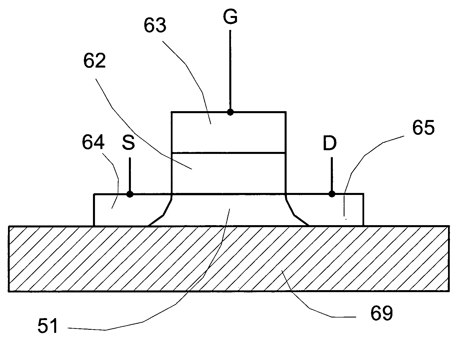
[0038] the present invention is shown in FIG. 3, illustrating a semiconductive metal oxide ferroelectric transistor. The gate stack of the present invention comprises a top gate electrode 63 and a ferroelectric film 62, positioning on a semiconductive metal oxide layer 51 disposed on a substrate 69, and disposed between the source 64 and drain 65 regions having a high concentration of opposite type impurity ions. The ferroelectric transistor is isolated by the isolation substrate 69. The conductive channel layer of the present invention transistor is fabricated with a semiconductive metal oxide such as In2O3 or RuO2. The semiconductive metal oxide in this example can be doped with p-type (n-type) impurities to form n-type (p-type) semiconductive metal oxide material.

[0039]FIG. 4 show the operation of an n-channel semiconductive metal oxide ferroelectric transistor. In FIG. 4A, when a positive voltage is applied to the gate electrode 63, polarization of the ferroelectric film 62 occu...

second embodiment

[0041] In the invention, a bottom gate electrode is included. Thus gate stack of the semiconductive metal oxide gate ferroelectric transistor comprises a top gate electrode 163, a ferroelectric film 162 and a bottom gate electrode 61 as shown in FIG. 5. The bottom electrode 61 is connected to the semiconductive metal oxide channel 51, and therefore the bottom electrode 61 is not electrically isolated, and would not be able to accumulate charges likes a floating gate. The charge retention time of this device is thus independent of the current flow through the ferroelectric thin film.

[0042] In alternate embodiments of the invention, a gate dielectric is included. Thus gate stack of the semiconductive metal oxide gate ferroelectric transistor comprises a top gate electrode 163, a ferroelectric film 162 and a gate dielectric 81 as shown in FIG. 6, or a top gate electrode 163, a ferroelectric film 162, a bottom electrode 61 and a gate dielectric 81 as shown in FIG. 7. The gate dielectric...


PUM

PropertyMeasurementUnit
thicknessaaaaaaaaaa
thicknessaaaaaaaaaa
thickaaaaaaaaaa

Abstract

The present invention discloses a novel transistor structure employing semiconductive metal oxide as the transistor conductive channel. By replacing the silicon conductive channel with a semiconductive metal oxide channel, the transistors can achieve simpler fabrication process and could realize 3D structure to increase circuit density. The disclosed semiconductive metal oxide transistor can have great potential in ferroelectric non volatile memory device with the further advantages of good interfacial properties with the ferroelectric materials, possible lattice matching with the ferroelectric layer, reducing or eliminating the oxygen diffusion problem to improve the reliability of the ferroelectric memory transistor. The semiconductive metal oxide film is preferably a metal oxide exhibiting semiconducting properties at the transistor operating conditions, for example, In2O3 or RuO2. The present invention ferroelectric transistor can be a metal-ferroelectric-semiconductive metal oxide FET having a gate stack of a top metal electrode disposed on a ferroelectric layer disposed on a semiconductive metal oxide channel on a substrate. Using additional layer of bottom electrode and gate dielectric, the present invention ferroelectric transistor can also be a metal-ferroelectric-metal (optional)-gate dielectric (optional)-semiconductive metal oxide FET.

Description

FIELD OF THE INVENTION [0001] This invention related generally to semiconductor device and nonvolatile memory transistor, and more particularly to ferroelectric gate transistor structures and methods of fabrication. BACKGROUND OF THE INVENTION [0002] Ferroelectric materials are composed of many randomly-distributed permanently polarized regions. Under the presence of an electric field, the regions with a polarization component in the direction of the electric field grow at the expense of the non-aligned regions so that a net polarization can result. If the electric field decreases, the polarization also decreases but at a slower rate so that even when the electric field becomes zero, a remnant polarization remains. This remnant polarization, existed under zero field condition (i.e., when power is turned off), is the basis of ferroelectric nonvolatile memory devices such as ferroelectric transistors. [0003] The ferroelectric transistor is typically a ferroelectric-gate-controlled sem...

Claims


Application Information

Patent Timeline
23 Feb 2006
Publication
US20060038242A1
IPC
H01L29/94; H01L29/76
CPC
H01L29/516; H01L29/66545; H01L29/7869; H01L29/78621; H01L29/66553
Inventors
HSU, SHENG TENG; LI, TINGKAI