Power MOSFET with recessed field plate

a power mosfet and field plate technology, applied in the direction of diodes, semiconductor devices, electrical apparatus, etc., can solve the problems of power mosfets becoming increasingly inconvenient to operate with satisfactory efficiency performance and power loss, and the variation of mesa width and hence breakdown voltag

Active Publication Date: 2008-03-27
MAXPOWER SEMICON INC
View PDF13 Cites 157 Cited by
  • Summary
  • Abstract
  • Description
  • Claims
  • Application Information

AI Technical Summary

Benefits of technology

[0007]FIG. 1 is a cross-sectional view of a conventional trench-type MOSFET.

Problems solved by technology

Furthermore, when these devices operate in the third quadrant, i.e. where the drain-body junction is forward-biased, charge is stored as a result of minority carrier injection, and this stored charge causes a delay in switching speed of the device.
Furthermore, in MOSFET 20 the deep and shallow trenches are not self-aligned, which causes variations in mesa widths and hence in breakdown voltages.
As the switching-speed requirements increase to 1 MHz and above, driven by new applications such as CPU voltage regulator module (VRM), power MOSFETs are becoming increasingly unable to operate with satisfactory efficiency performance and power loss.

Method used


Image

  • Power MOSFET with recessed field plate
  • Power MOSFET with recessed field plate
  • Power MOSFET with recessed field plate

Examples


Embodiment Construction

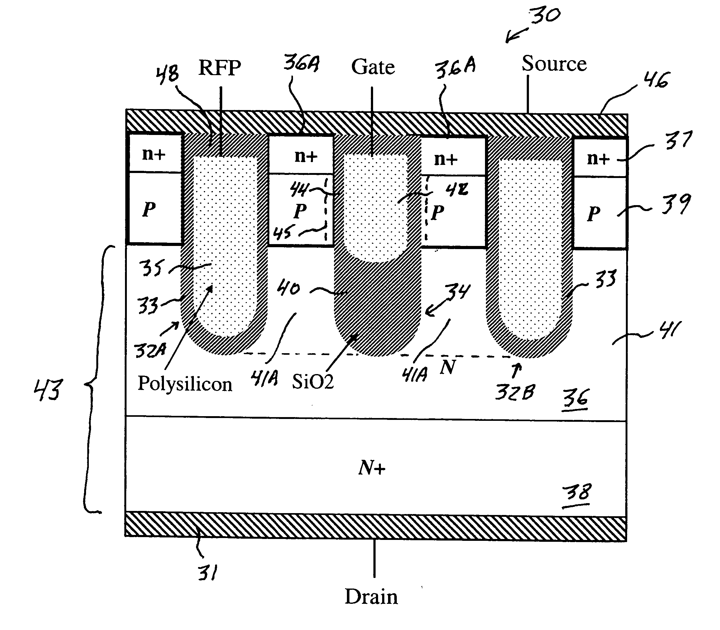
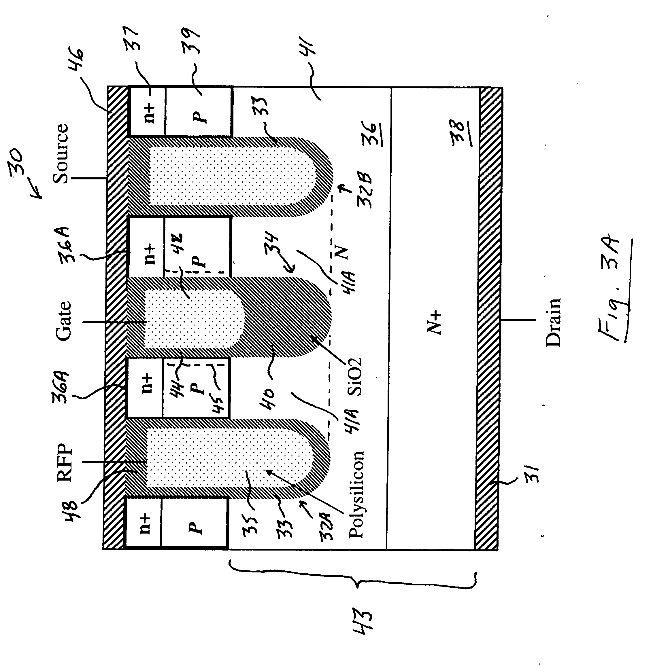
[0030]A basic cell of an n-channel MOSFET 30 in accordance with this invention is shown in FIG. 3A. MOSFET 30 is formed in a semiconductor die comprising an n-type epitaxial layer 36 that is grown over a heavily doped n+ substrate 38. MOSFET 30 includes recessed field plate (RFP) trenches 32A and 32B located on either side a gate trench 34 in the n-type epitaxial layer 36. Unlike the trenches in the MOSFET 20 shown in FIG. 2, the thick bottom oxide of the gate trench 34 extends to substantially the same depth as the RFP trenches 32A and 32B. Furthermore, the RFP trenches 32A and 32B and the gate trench 34 are preferably formed in the same processing step and therefore are self-aligned (i.e., the RFP trenches 32A and 32B are equally spaced from gate trench 34 regardless of processing and alignment variations), and RFP trenches 32A and 32B and gate trench 34 are of equal or substantially equal depth (e.g., the respective depths of RFP trenches 32A and 32B are within + / −10%, or prefera...


PUM


Abstract

A trench MOSFET contains a recessed field plate (RFP) trench adjacent the gate trench. The RFP trench contains an RFP electrode insulated from the die by a dielectric layer along the walls of the RFP trench. The gate trench has a thick bottom oxide layer, and the gate and RFP trenches are preferably formed in the same processing step and are of substantially the same depth. When the MOSFET operates in the third quadrant (with the source/body-to-drain junction forward-biased), the combined effect of the RFP and gate electrodes significantly reduces in the minority carrier diffusion current and reverse-recovery charge. The RFP electrode also functions as a recessed field plates to reduce the electric field in the channel regions when the MOSFET source/body to-drain junction reverse-biased.

Description

CROSS-REFERENCE TO RELATED APPLICATIONS[0001]This application claims the priority of Provisional Application No. 60 / 847,551, filed Sep. 27, 2006, which is incorporated herein by reference in its entirety.BACKGROUND OF THE INVENTION[0002]Power MOSFETs are widely used as switching devices in many electronic applications. In order to minimize conduction power loss it is desirable that power MOSFETs have a low specific on-resistance, which is defined as the product of the on-resistance (Ron) of the MOSFET multiplied by the active die area (A) of the MOSFET (Ron*A). A trench-type MOSFET, as shown in the schematic cross-sectional view of a MOSFET 10 in FIG. 1, provides a low specific on-resistance because of its high packing density or number of cells per unit area. As the cell density increases, the associated capacitances, such as the gate-to-source capacitance (Cgs), the gate-to-drain capacitance (Cgd), and the drain-to-source capacitance (Cds), also increase. In many switching applica...

Claims


Application Information

Patent Timeline
Patent Type & Authority Applications(United States)
IPC IPC(8): H01L29/78H01L21/336
CPCH01L21/26586H01L29/0696H01L29/1095H01L29/407H01L29/7813H01L29/42368H01L29/66734H01L29/7808H01L29/7809H01L29/41766H01L2924/13091
Inventor DARWISH, MOHAMED N.
Owner MAXPOWER SEMICON INC
Why Eureka
Try Eureka