Deposition On A Nanowire Using Atomic Layer Deposition

Active Publication Date: 2012-12-27
ALSEPHINA INNOVATIONS INC
View PDF3 Cites 7 Cited by
  • Summary
  • Abstract
  • Description
  • Claims
  • Application Information

AI Technical Summary

Benefits of technology

[0011]The GAA structure has potential for improving performance of extremely-scaled FETs. In addition,

Problems solved by technology

Semiconductors and integrated circuit chips have become ubiquitous within many products due to their continually decreasing cost and size.

Method used


Image

  • Deposition On A Nanowire Using Atomic Layer Deposition
  • Deposition On A Nanowire Using Atomic Layer Deposition
  • Deposition On A Nanowire Using Atomic Layer Deposition

Examples


Embodiment Construction

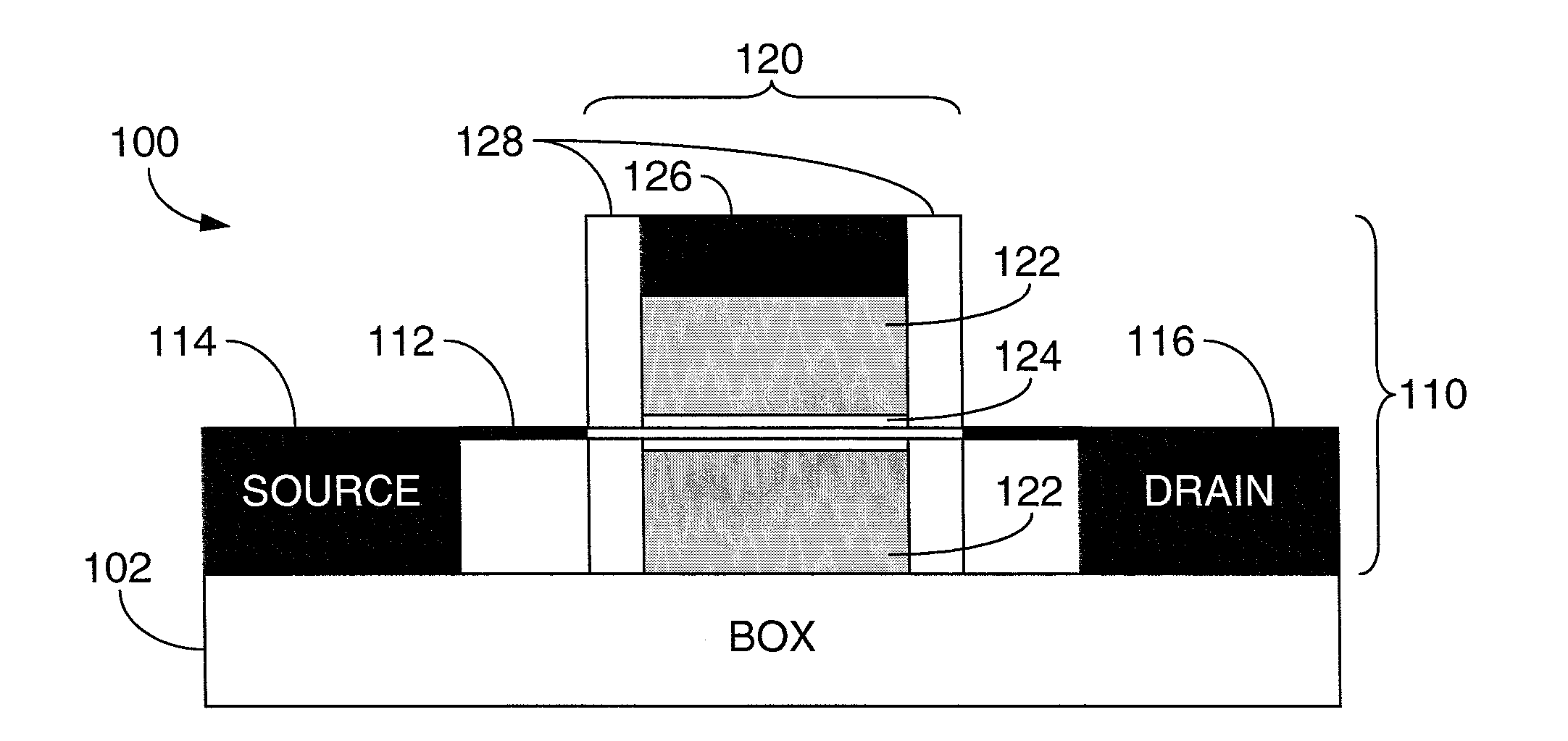
[0027]It is desirable to reduce the resistance of the nanowire linking the source / drain pads and the channel. In furtherance of this goal, one can form a silicide on the nanowire, for example, by sputtering or evaporating a metal onto the nanowire and subsequently performing an anneal (e.g., a rapid thermal anneal or RTA).

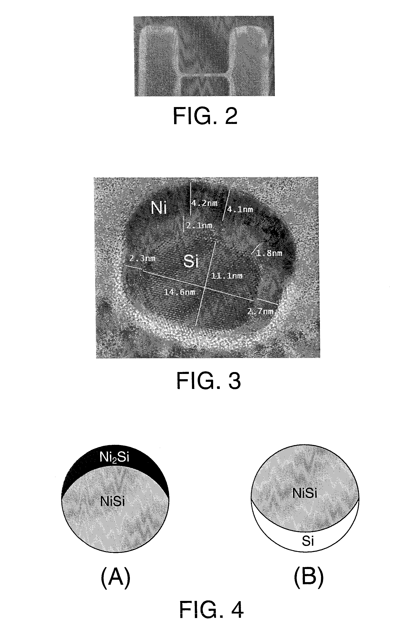
[0028]FIG. 2 shows an exemplary Si nanowire suspended between two pads (e.g., contacts, source / drain pads). When a metal film is sputtered or evaporated to a suspended Si nanowire (such as the one shown in FIG. 2) for the silicidation process, it is very difficult to obtain full coverage (e.g., completely surrounding the nanowire). As a result, when silicide is formed from sputtering or evaporating Ni onto a suspended Si nanowire, two situations commonly arise. FIG. 3 shows a transmission electron microscope (TEM) cross-section for Ni film coverage on a suspended Si nanowire as deposited with sputtering (i.e., before RTA and formation of silicide). If the Ni covera...


PUM


Abstract

A semiconductor device includes a substrate, a nanowire, a first structure, and a second structure. The nanowire is suspended between the first structure and the second structure, where the first structure and the second structure overly the substrate, where the nanowire includes a layer on a surface of the nanowire, where the layer includes at least one of silicide and carbide, where the layer has a substantially uniform shape.

Description

CROSS-REFERENCE TO RELATED APPLICATIONS[0001]This is a continuation of U.S. patent Ser. No. 13 / 013,067, filed on Jan. 25, 2011, which is incorporated by reference in its entirety.TECHNICAL FIELD[0002]The exemplary embodiments of this invention relate generally to semiconductor structures and, more specifically, relate to deposition on a nanowire structure.BACKGROUND[0003]This section endeavors to supply a context or background for the various exemplary embodiments of the invention as recited in the claims. The content herein may comprise subject matter that could be utilized, but not necessarily matter that has been previously utilized, described or considered. Unless indicated otherwise, the content described herein is not considered prior art, and should not be considered as admitted prior art by inclusion in this section.[0004]Semiconductors and integrated circuit chips have become ubiquitous within many products due to their continually decreasing cost and size. In the microelec...

Claims


Application Information

Patent Timeline
IPC IPC(8): H01L29/775H01L21/30B82Y99/00
CPCH01L21/845B82Y10/00H01L29/0673H01L29/47H01L29/6675H01L29/7839Y10S977/762Y10S977/938B82Y30/00B82Y40/00H01L51/0048H01L51/0516H01L51/0558H01L51/057H01L27/1211H01L21/84H01L29/42392H01L27/1203H10K85/221H10K10/468H10K10/484H10K10/491
Inventor GUO, DECHAOLI, ZHENGWENWANG, KEJIAZHANG, ZHENZHU, YU
Owner ALSEPHINA INNOVATIONS INC
Why Eureka
Try Eureka