Display device, thin-film transistor used for display device, and method of manufacturing thin-film transistors

a technology of thin-film transistors and display devices, which is applied in the direction of semiconductor devices, basic electric elements, electrical appliances, etc., can solve the problems of undetected deterioration of the characteristics of thin-film transistors, low mobility of amorphous silicon films, and small on-current, so as to increase the number of processing steps and stable characteristics

Inactive Publication Date: 2013-01-03
JOLED INC
View PDF2 Cites 1 Cited by
  • Summary
  • Abstract
  • Description
  • Claims
  • Application Information

AI Technical Summary

Benefits of technology

[0013]As described above, the present invention provides thin-film transistors with stable characteristics without greatly increasing the number of processing steps.

Problems solved by technology

Conventionally, as a channel-forming region of such a thin-film transistor, an amorphous (non-crystalline) silicon film for instance has been used; however, an amorphous silicon film has low mobility and resultantly the on-current is small.
To use this crystallized silicon film for a thin-film transistor, after forming an ohmic contact layer on the channel-forming region, when processing the ohmic contact layer, damage to the channel-forming region remains, which undesirably deteriorate the characteristics of the thin-film transistor.
In this conventional configuration, however, an ohmic contact layer directly contacts a crystallized silicon film, causing an electric field to concentrate between them, which undesirably increases the off-current.

Method used


Image

  • Display device, thin-film transistor used for display device, and method of manufacturing thin-film transistors
  • Display device, thin-film transistor used for display device, and method of manufacturing thin-film transistors
  • Display device, thin-film transistor used for display device, and method of manufacturing thin-film transistors

Examples


Embodiment Construction

Exemplary Embodiment

[0027]Hereinafter, a description is made of a thin-film transistor (hereinafter sometimes abbreviated as TFT), and a method of manufacturing TFTs, according to an embodiment of the present invention with reference to the related drawings.

[0028]First, a description is made of a display device according to the embodiment of the present invention, taking an organic EL display device as an example.

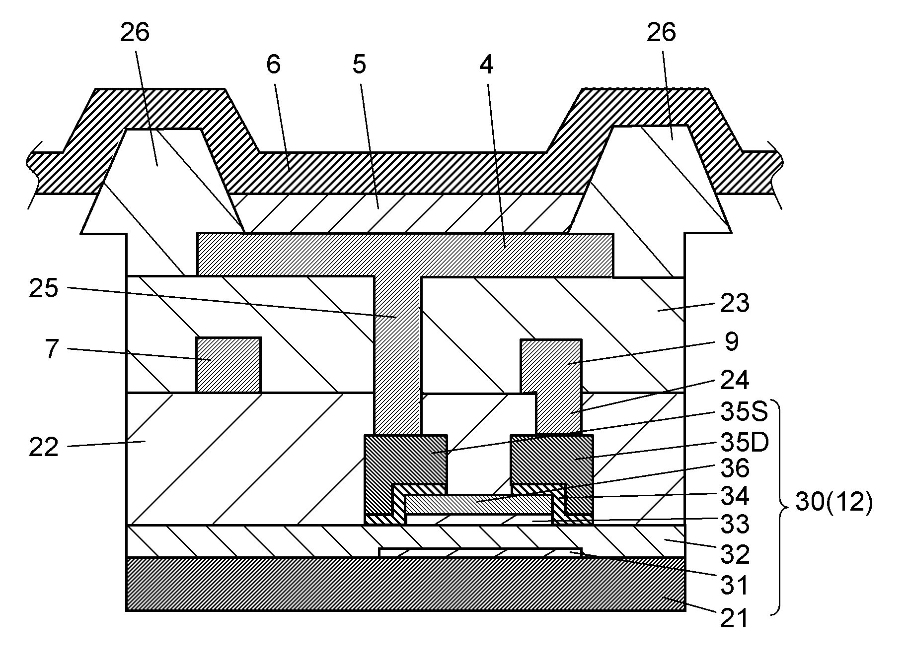
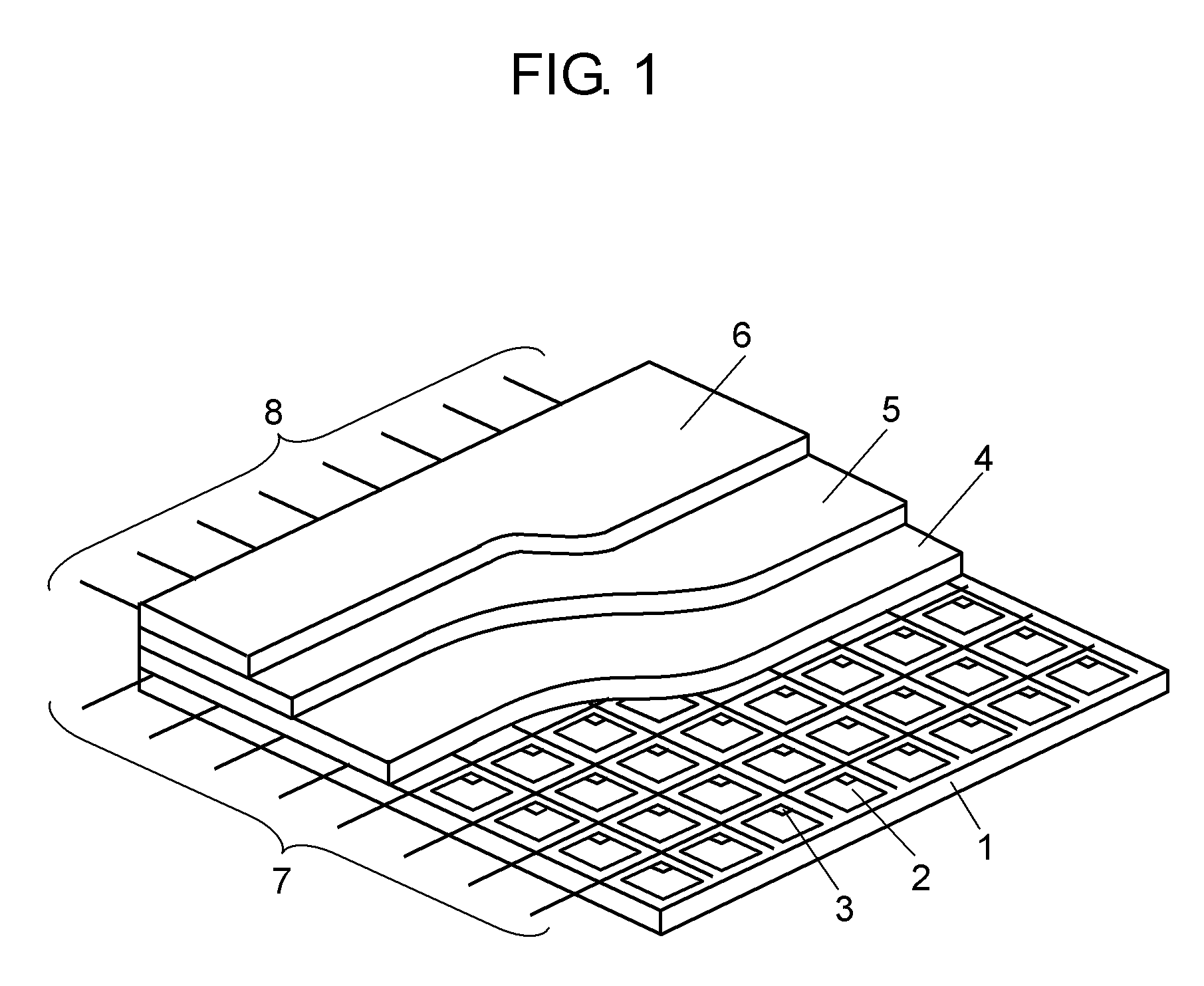
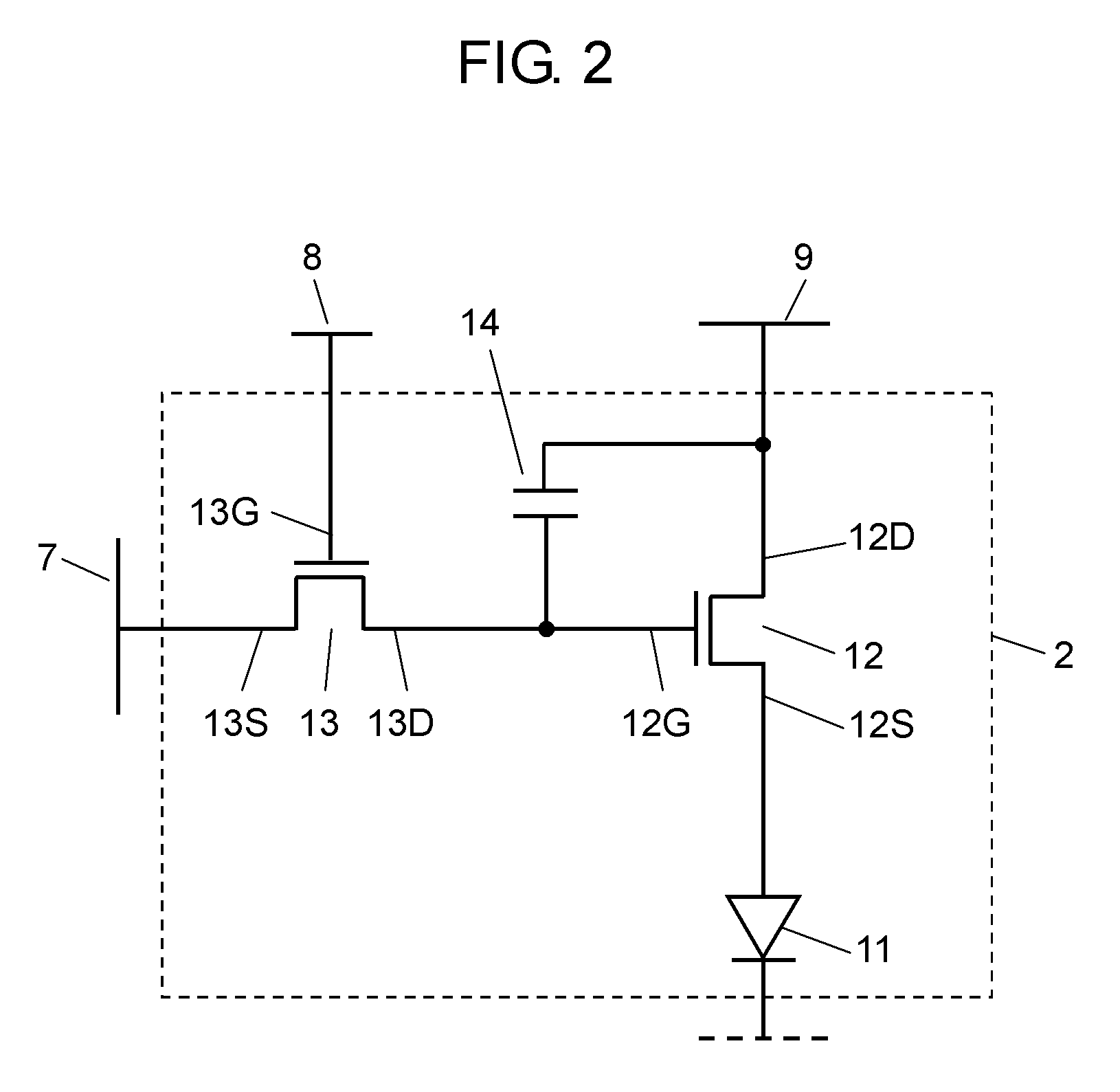
[0029]FIG. 1 is a partial cutaway perspective view of an organic EL display device as a display device according to the embodiment of the present invention, showing an outline structure of the organic EL display device. As shown in FIG. 1, the organic EL display device includes active matrix substrate 1; pixels 2 arranged in a matrix on active matrix substrate 1; pixel circuits 3 connected to pixels 2, arranged in an array on active matrix substrate 1; an EL element composed of electrode 4 as a positive electrode, organic EL layer 5, and electrode 6 as a negative electrode,...


PUM


Abstract

A thin-film transistor used for a display device includes a gate electrode formed on an insulating substrate; a gate insulating film formed on the substrate so as to cover the gate electrode; a semiconductor layer composed of first semiconductor layer and second semiconductor layer formed on the gate insulating film; an ohmic contact layer formed on the semiconductor layer; and a source electrode and a drain electrode formed on the ohmic contact layer so as to be spaced from each other. The transistor further includes an etching stopper made of spin-on glass (SOG) on a channel-forming region of the semiconductor layer.

Description

TECHNICAL FIELD[0001]The present invention relates to a display device such as an organic electroluminescence (EL) display device, to a thin-film transistor used for the display device, and to a method of manufacturing thin-film transistors.BACKGROUND ART[0002]In recent years, organic EL display devices including current-driven organic EL elements have been receiving attention as a next-generation display device. Among them, an active-matrix-driven organic EL display device includes a field-effect transistor. As such a field-effect transistor, there is known a thin-film transistor where a semiconductor layer provided on a substrate with an insulating surface becomes a channel-forming region.[0003]A thin-film transistor used for an active-matrix-driven organic EL display device requires at least a switching transistor for controlling timing (e.g. turning on and off) of driving an organic EL element; and a drive transistor for controlling the amount of light emitted from the organic E...

Claims


Application Information

Patent Timeline
Patent Type & Authority Applications(United States)
IPC IPC(8): H01L27/15H01L21/336
CPCH01L29/41733H01L29/66765H01L27/1248H01L29/78696H01L29/78606H10K59/1213
Inventor SATOH, EIICHIKAWACHI, GENSHIROUKAWASHIMA, TAKAHIRO
Owner JOLED INC
Why Eureka
Try Eureka