Semiconductor Device

a technology of semiconductor devices and semiconductors, applied in the direction of semiconductor devices, basic electric elements, electrical equipment, etc., can solve the problems of difficult to realize circuit operation conforming design specifications, difficult to use gate electrodes as masks, and difficult to use this step in the manufacturing of integrated circuits, etc., to achieve the effect of improving the density of output curren

Inactive Publication Date: 2013-01-03
HITACHI LTD
View PDF2 Cites 8 Cited by
  • Summary
  • Abstract
  • Description
  • Claims
  • Application Information

AI Technical Summary

Benefits of technology

[0017]Stable circuit operations conforming design specifications can be realized and the density of an output current can be improved by suppressing variations in the channel length ...

Problems solved by technology

However, this manufacturing step requires application of large thermal load after the gate electrodes are formed; therefore, it is difficult to use this step in manufacturing of an integrated circuit for which consolidation with a fine CMOS is premised.
However, in this case, the gate electrode cannot be used as a mask; therefore, for example, different masks are respectively used as a mask for forming the body region that determines a threshold voltage and as a mask for forming a source region, and the relative positions of the masks are mutually misaligned.
When the threshold voltage is varied, it becomes difficult to realize circuit operations conforming design specifications.
Particularly, variation in the channel length means variation in chann...

Method used


Image

  • Semiconductor Device
  • Semiconductor Device
  • Semiconductor Device

Examples


first embodiment

Device Structure of Medium / High-Voltage MOSFET

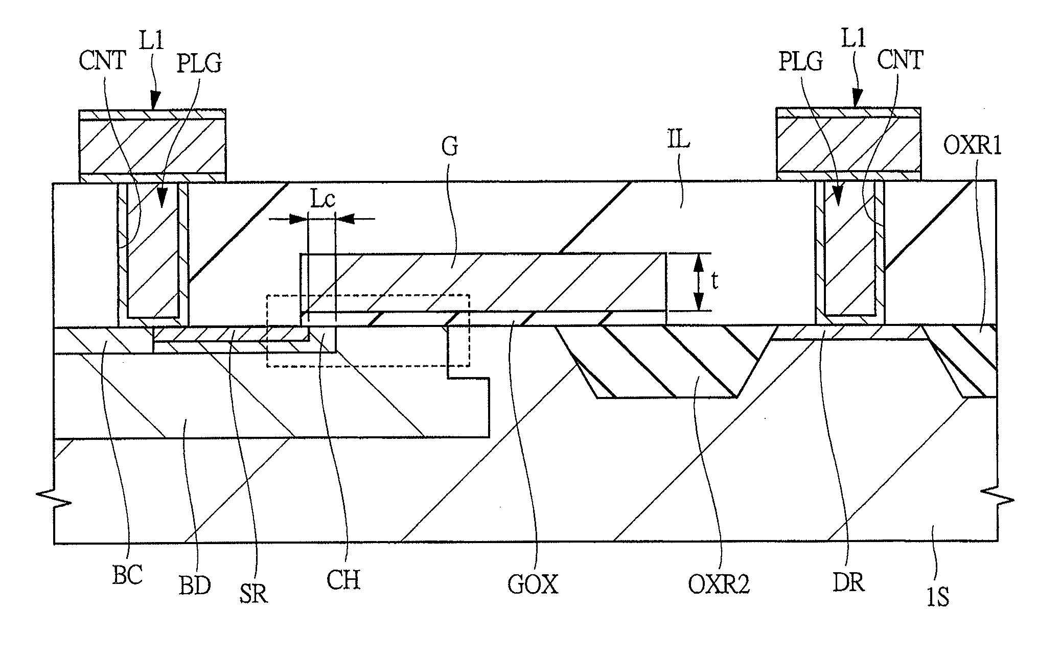
[0048]A device structure of a medium / high-voltage MOSFET in a present first embodiment will be described with reference to the drawings. First, in the present specification, for example, a MOSFET having a breakdown voltage between a source region and a drain region of 20 V to 200 V-class is assumed as an example of the medium / high-voltage MOSFET to give explanation. However, the present invention is not limited thereto, and the device structure in the present first embodiment can be applied to various MOSFETs.

[0049]FIG. 1 is a cross-sectional view showing a device structure of the medium / high-voltage MOSFET in the present first embodiment. As shown in FIG. 1, first, the medium / high-voltage MOSFET in the present first embodiment is formed on a semiconductor substrate 1S to which an n-type impurity such as phosphorous (P) or arsenic (As) is introduced. Specifically, an oxide-film region OXR1 is formed in an element formation surface (surfa...

second embodiment

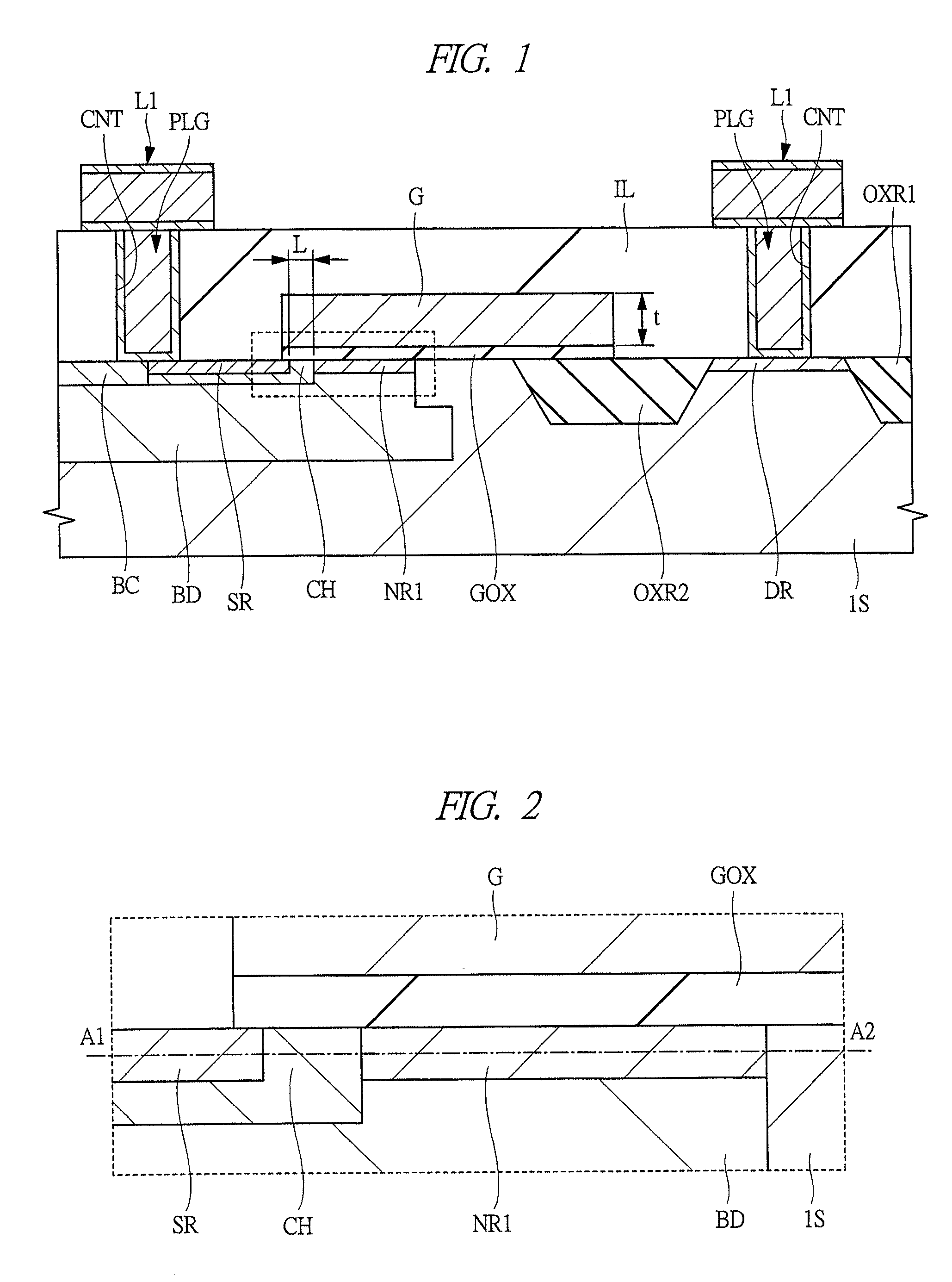
[0113]In the above-described first embodiment, the example in which the n-type semiconductor region NR1 having an impurity concentration higher than that of the semiconductor substrate 1S is provided in the region in which the channel region CH is not formed in the region immediately below the gate electrode G has been described. However, in the present second embodiment, an example in which the above-described n-type semiconductor region NR1 is not provided will be described. The device structure of a medium / high-voltage MOSFET in the present second embodiment is substantially similar to the device structure of the medium / high-voltage MOSFET in the above-described first embodiment; therefore, different points will be mainly described below.

Characteristics of the Present Second Embodiment

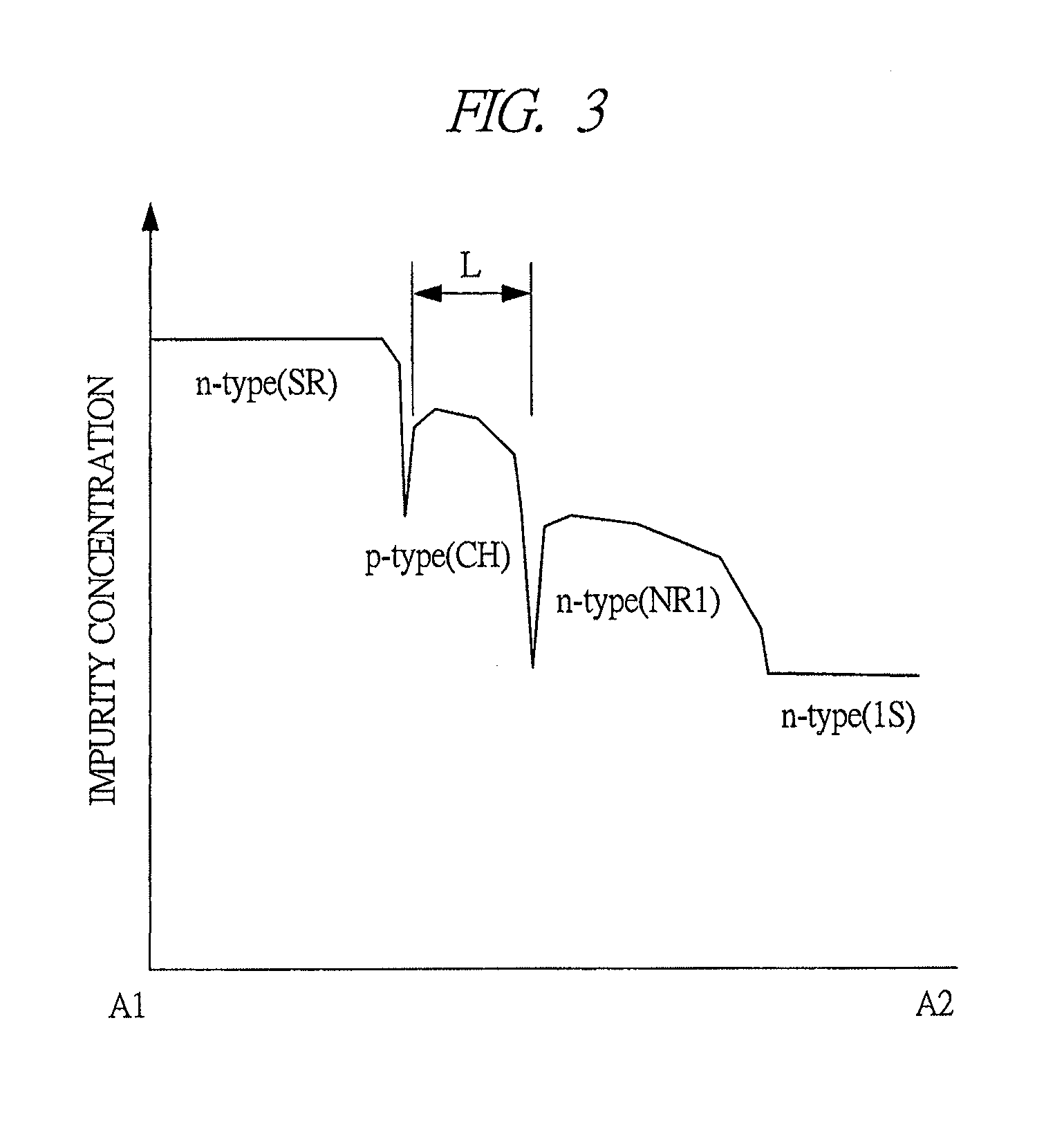
[0114]FIG. 13 is a cross-sectional view showing the device structure of the medium / high-voltage MOSFET in the present second embodiment. Also in the present second embodiment, as well as the above-d...

third embodiment

[0134]In the present third embodiment, application examples of the medium / high-voltage MOSFETs described in the above-described first embodiment and the second embodiment will be described. FIG. 24 is a drawing showing an example in which the medium / high-voltage MOSFET of the present invention is applied to an output-stage circuit of an integrated circuit in which a digital circuit and an analog circuit are consolidated. In FIG. 24, the output-stage circuit OC has a configuration in which a p-channel-type MOSFET QH and an n-channel-type MOSFET QL of the present invention are connected in series between a power source electric potential VH and a reference electric potential GND. In this case, the p-channel-type MOSFET QH is connected to the power source electric potential VH side, and the n-channel-type MOSFET QL is connected to the reference electric potential GND side. A connection node (connecting point) between the p-channel-type MOSFET QH and the n-channel-type MOSFET QL serves ...


PUM


Abstract

The present invention relates to an integrated circuit (semiconductor device) for which consolidation of a fine CMOS and a medium/high-voltage MOSFET is assumed to be carried out. A feature of the present invention is a small width (channel length) of a channel region CH. Specifically, when the width of the channel region planarly overlapped with a gate electrode is “L” and the thickness of the gate electrode is “t”, the channel region is formed to have the width of the channel region being larger than or equal to ⅕ times the thickness t of the gate electrode and smaller than or equal to the thickness t. Thus, the width L of the channel region can be reduced, and variations in the threshold voltage can be reduced.

Description

CROSS-REFERENCE TO RELATED APPLICATION[0001]The present application claims priority from Japanese Patent Application No. 2011-144130 filed on Jun. 29, 2011 the content of which is hereby incorporated by reference into this application.TECHNICAL FIELD OF THE INVENTION[0002]The present invention relates to a semiconductor device and particularly relates to technique effective in application to a semiconductor device including a field-effect transistor represented by MOSFET (Metal Oxide Semiconductor Field Effect Transistor).BACKGROUND OF THE INVENTION[0003]Japanese Patent Application Laid-Open Publication No. H11-266018 describes technique by which the on-state current of a lateral IGBT can be increased. Specifically, an n-type relay layer is formed in a surface of an n−-type drift layer so as to be opposed to an n+-type source layer. The width of a large-resistance channel region can be reduced by providing this n-type relay layer. The on-state resistance of the lateral IGBT can be r...

Claims


Application Information

Patent Timeline
IPC IPC(8): H01L29/78
CPCH01L21/26586H01L21/266H01L29/0653H01L29/7816H01L29/1045H01L29/1095H01L29/66681H01L29/0878H01L29/66659H01L29/7835
Inventor SHIRAKAWA, SHINJISAKANO, JUNICHI
Owner HITACHI LTD
Why Eureka
Try Eureka