Apparatus and method for measuring degradation of CMOS VLSI elements

a technology of cmos and vlsi elements, applied in the direction of measurement devices, instruments, semiconductor operation lifetime testing, etc., can solve the problems of physical degradation of mos devices, signs of degradation, and transistors (mosfets) subject to physical effects that degrade operating characteristics

Active Publication Date: 2013-01-17
TAIWAN SEMICON MFG CO LTD
View PDF2 Cites 43 Cited by
  • Summary
  • Abstract
  • Description
  • Claims
  • Application Information

AI Technical Summary

Benefits of technology

[0017]It would be advantageous to provide a circuit and technique that permits the effects of degradation effects, including HCI, NBTI, PBTI, TDDB to be assessed in isolation from one another. It would also be advantageous to assess these effects while minimizing the need for plural ring oscillators with calibration requirements and switching complication on a large integrated circuit area.

Problems solved by technology

Metal oxide semiconductor field effect transistors (MOSFET) are subject to physical effects that degrade operating characteristics, temporarily with stress or permanently due to accumulating effects of stress and / or operational conditions.
Although durable and long-lived as a class of devices, physical degradation of MOS devices occurs, and is a concern, particularly as the devices are scaled to very small dimensions in densely arranged integrated circuit designs.
Signs of degradation may include an increase in the threshold voltage of a device, progressively greater conductivity through the gate dielectric, changes in on or off current levels, etc.
Damage to the oxide affects its characteristics, especially current leakage through the dielectric.
Increased current along such lower resistance conductive paths causes heating.
With progressive TDDB degradation, the device continues to operate while its specifications deteriorate, unless or until a conductive path shorts through the oxide layer, making the gate inoperable.
However, in some designs, tradeoffs are made, and perhaps size is scaled down more than drive voltage, leading to added stress.
When the degradation of particular elements causes its operational characteristics to fall out of the range for which the circuit was designed, the integrated circuit may fail.
As stated above, one of the effects of degradation is an increase in the threshold voltage of the degraded MOS device.
Degradation of the inverter transistors in the stressed ring oscillator in Kim tends to lower the operating frequency of the oscillator.
Also, generally applying stress to all the cascaded inverters of the stressed ring oscillator does not permit one to distinguish between the effects of NBTI, PBTI, HCI, TDDB, etc.
This causes the outputs of the cascaded DRIVE_ROSC inverters to reverse bias the gate dielectrics of the BTI_ROSC inverters, and causes BTI stress.
However this test arrangement is not able to test for other degradation effects, notably TDDB.

Method used


Image

  • Apparatus and method for measuring degradation of CMOS VLSI elements
  • Apparatus and method for measuring degradation of CMOS VLSI elements
  • Apparatus and method for measuring degradation of CMOS VLSI elements

Examples


Embodiment Construction

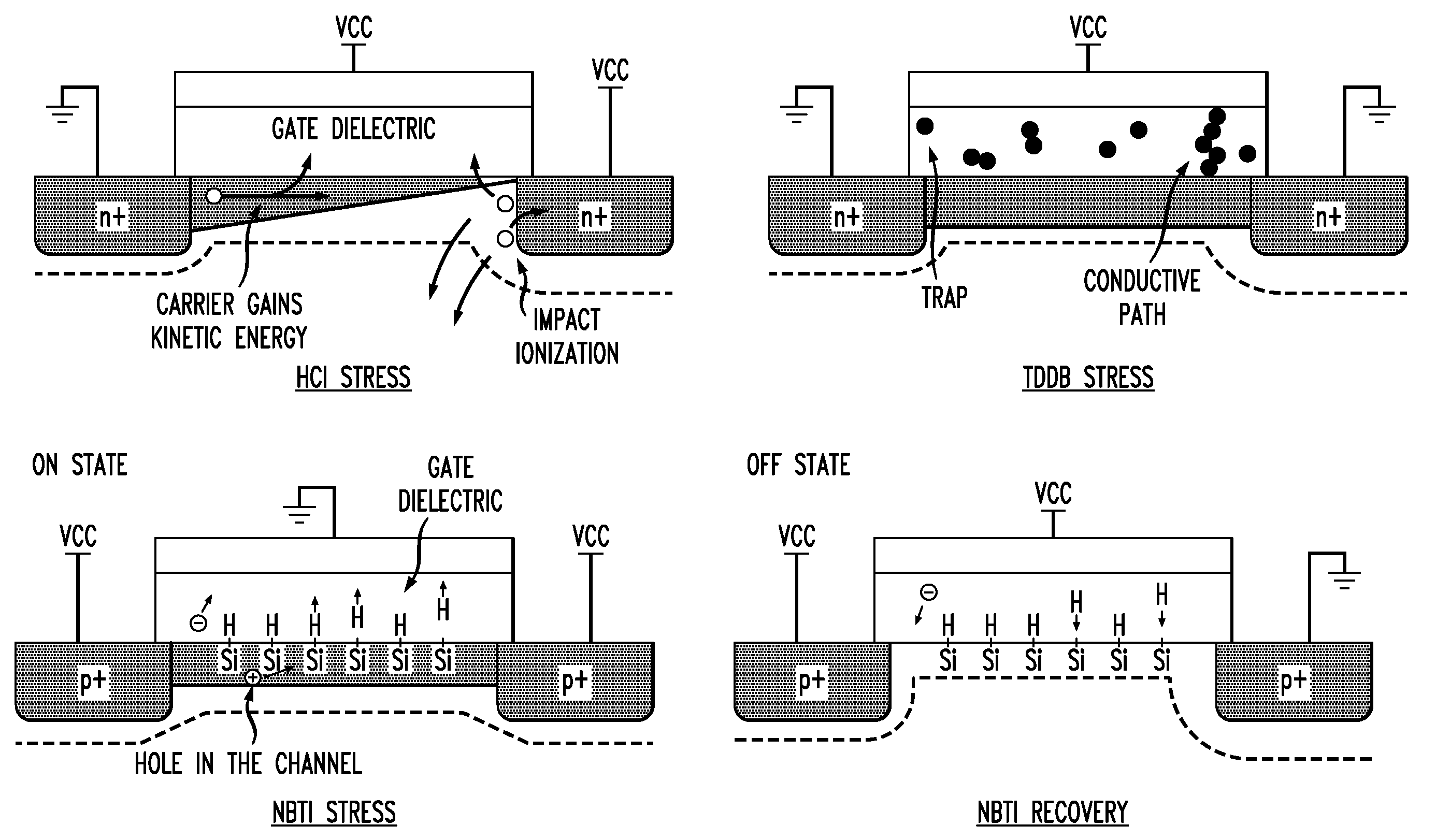
[0041]FIG. 1 is a figurative comparison of cross sections through CMOS elements and compares how the presence or absence of source / drain bias voltages and gate / substrate input voltages contribute to certain types of degradation in NMOS and PMOS devices.

[0042]A source / drain voltage in an NMOS device can impart kinetic energy to electrons as charge carriers, leading to injection into the gate dielectric of carriers of higher energy or carriers that result from ionization. This is known as hot carrier injection (HCI) and causes deterioration of operating characteristics including elevation of device threshold voltage.

[0043]Apart from source / drain voltage, a positive potential difference between the gate and substrate can cause the migration of charge carriers into the gate dielectric, producing charge traps that accumulate over time and can cause paths of relatively lower resistance through the dielectric, leading to localized heating. This effect is time dependent dielectric breakdown...


PUM


Abstract

The reliability of an integrated circuit is inferred from the operational characteristics of sample metal oxide semiconductor (MOS) devices switchably coupled to drain/source bias and gate input voltages that are nominal, versus voltage and current conditions that elevate stress and cause temporary or permanent degradation, e.g., hot carrier injection (HCI), bias temperature instability (BTI, NBTI, PBTI), time dependent dielectric breakdown (TDDB). The MOS devices under test (preferably both PMOS and NMOS devices tested concurrently or in turn) are configured as current sources in the supply of power to a ring oscillator having cascaded inverter stages, thereby varying the oscillator frequency as a measure of the effects of stress on the devices under test, but without elevating the stress applied to the inverter stages.

Description

BACKGROUND[0001]This disclosure relates to assessing and forecasting the degradation of PMOS and NMOS circuit elements by comparing the operating characteristics of elements when stressed by voltage biasing conditions, versus operating characteristics of the same or other similar elements when not stressed.[0002]Metal oxide semiconductor field effect transistors (MOSFET) are subject to physical effects that degrade operating characteristics, temporarily with stress or permanently due to accumulating effects of stress and / or operational conditions. In digital integrated circuits, the devices typically are provided in complementary MOS pairs with an NMOS element and a PMOS element coupled in series across a potential difference. One complementary element is conductive and the other nonconductive in any given logic state, which situation is reversed when switched to the other logic state. Although durable and long-lived as a class of devices, physical degradation of MOS devices occurs,...

Claims


Application Information

Patent Timeline
Patent Type & Authority Applications(United States)
IPC IPC(8): G01R31/26
CPCG01R31/2642G01R31/31924
Inventor LAI, FANG-SHI JORDANLU, CHIH-CHENGLIN, YUNG-FUHSUEH, HSU-FENGCHANG, CHIN-HAOWENG, CHENG YENMHALA, MANOJ M.
Owner TAIWAN SEMICON MFG CO LTD
Why Eureka
Try Eureka