Semiconductor device and method of adjusting an impedance of an output buffer

a technology of impedance adjustment and output buffer, which is applied in the direction of pulse technique, voltage/temperature variation compensation, reliability increasing modifications, etc., can solve the problems of increasing wiring area, increasing chip size, increasing chip size, etc., and achieves increasing chip size, increasing wiring area, and increasing chip size

Inactive Publication Date: 2013-01-17
LONGITUDE SEMICON S A R L
View PDF6 Cites 42 Cited by
  • Summary
  • Abstract
  • Description
  • Claims
  • Application Information

AI Technical Summary

Benefits of technology

[0007]However, the impedance control circuit disclosed in Patent Document 1 outputs, in parallel, a plurality of bits of impedance control information for use in adjusting the impedance of the output buffer and therefore requires a plurality of wires corresponding in number to the bits. This results in an increase in wiring area and an increase in chip size. Particularly, in an edge pad structure which has data terminals DQ for outputting data from an output buffer and ZQ terminals both of which are arranged on opposite sides, respectively, a plurality of wires extend between the opposite sides. In this case, there arises a problem that the wiring area at a central portion of the chip is enlarged and, as a result, brings about an increase in chip size.

Problems solved by technology

This results in an increase in wiring area and an increase in chip size.
In this case, there arises a problem that the wiring area at a central portion of the chip is enlarged and, as a result, brings about an increase in chip size.

Method used


Image

  • Semiconductor device and method of adjusting an impedance of an output buffer
  • Semiconductor device and method of adjusting an impedance of an output buffer
  • Semiconductor device and method of adjusting an impedance of an output buffer

Examples


first embodiment

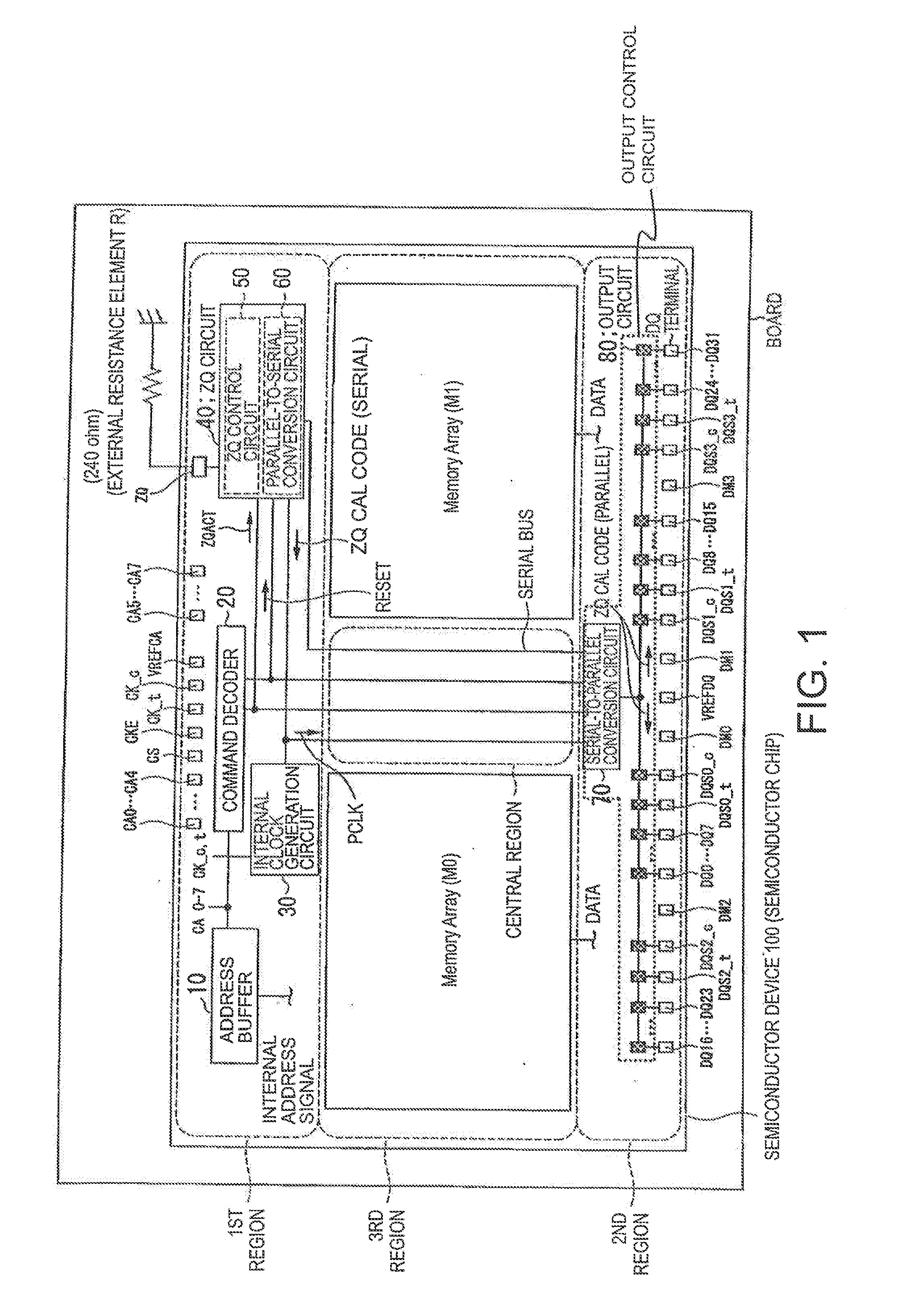
[0022]FIG. 1 shows a schematic structure of a semiconductor device 100 according to this invention. Herein, the illustrated semiconductor device 100 is an example of an SDRAM (synchronous dynamic random access memory) which operates synchronously with a clock signal supplied from the outside. Although the structure of the DRAM is used in this embodiment, this invention is not limited thereto and may be applied to a semiconductor memory (SRAM (Static RAM), PRAM (Phase Change RAM), flash memory, or the like) other than the DRAM or may be applied to a controller other than the memory.

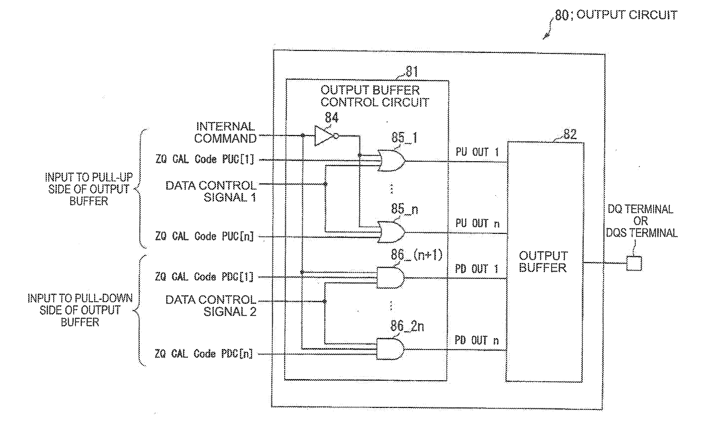
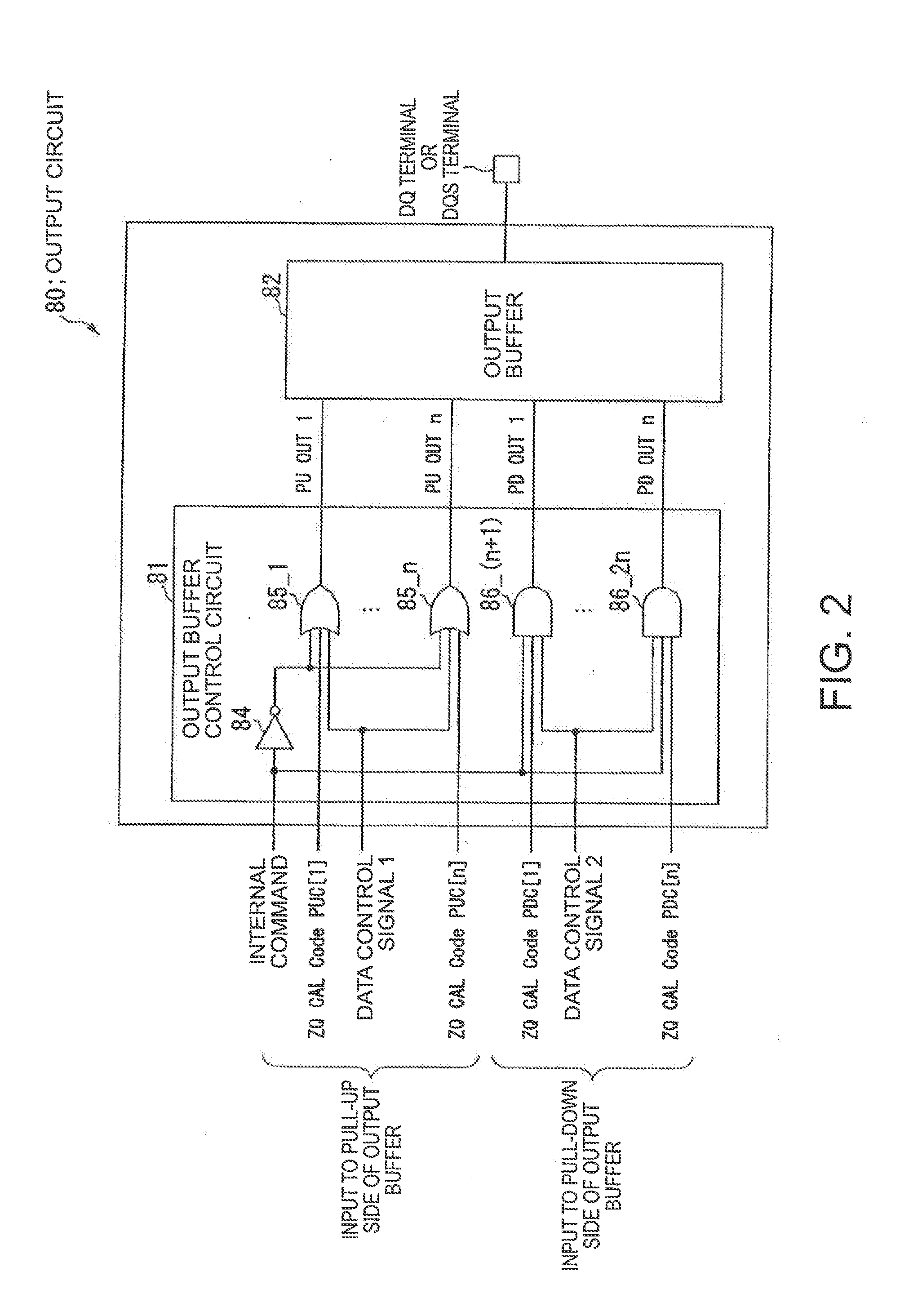
[0023]As shown in FIG. 1, the semiconductor device 100 (semiconductor chip) has a first region, a second region, and a third region and circuit blocks are respectively formed in these regions. The circuit blocks shown in FIG. 1 are formed on the same semiconductor chip made of single-crystal silicon. Each circuit block is formed by a plurality of transistors such as PMOS transistors (p-channel MOS transist...

second embodiment

[0158]Referring to FIG. 8, a semiconductor device 100 according to this invention is similar in structure and operation to that illustrated in FIG. 1 except that PUC[1] to PUC[n] and PDC[1] to PDC[n]) which form ZQ CAL Code are serially transferred through individual buses, namely, the serial bus and an additional bus, as shown in FIG. 8. With this structure also, it is possible to reduce the number of signal wires arranged within the third region of the semiconductor device 100.


PUM


Abstract

A semiconductor device has a ZQ circuit (40) which generates impedance control information and an output buffer having an impedance controlled in response to the impedance control information. A plurality of control bits constituting the impedance control information are serially transferred from the ZQ circuit.

Description

[0001]This application is based upon and claims the benefit of priority from Japanese patent application No. 2011-153666, filed on Jul. 12, 2011, the disclosure of which is incorporated herein in its entirety by reference.TECHNICAL FIELD[0002]This invention relates to a semiconductor device including an impedance control circuit and to a method of adjusting an impedance of an output buffer.BACKGROUND ART[0003]In recent years, data transfer between semiconductor devices (e.g. between a CPU and a memory) requires a higher data transfer rate. For the purpose of further increasing the data transfer rate, the amplitudes of input and output signals have been reduced more and more. When the amplitudes of input and output signals are reduced, the accuracy required for the impedance of an output buffer becomes stricter in order to output a signal with an exact amplitude.[0004]The impedance of the output buffer not only varies depending on the process condition in the manufacture, but changes...

Claims


Application Information

Patent Timeline
Patent Type & Authority Applications(United States)
IPC IPC(8): H03K19/003
CPCH03K19/018585H03K19/00369
Inventor HARAGUCHI, YOSHINORI
Owner LONGITUDE SEMICON S A R L
Why Eureka
Try Eureka