

Measurement apparatus, exposure apparatus, and method of manufacturing device
a technology of exposure apparatus and measurement apparatus, which is applied in the direction of photomechanical apparatus, focusing aids, instruments, etc., can solve the problems of difficult to accurately measure the surface position of the substrate, chip defects may be produced, and measurement errors, etc., to achieve accurate obtaining the physical information of an object
- Summary
- Abstract
- Description
- Claims
- Application Information
AI Technical Summary
Benefits of technology
Problems solved by technology
Method used
Image

Examples
first embodiment
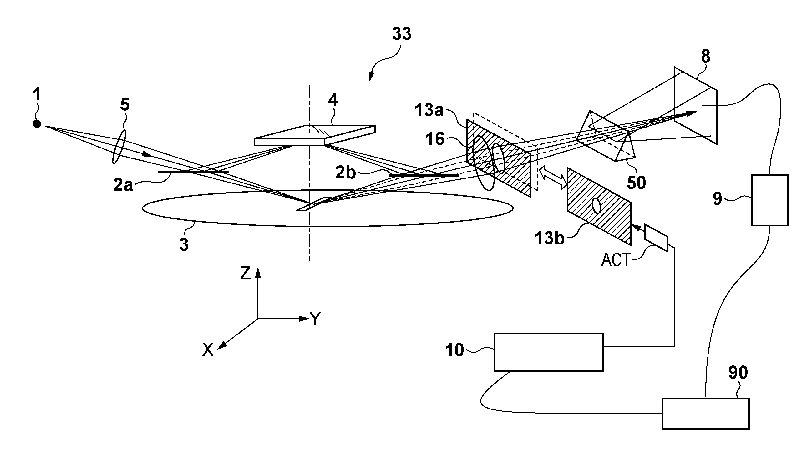
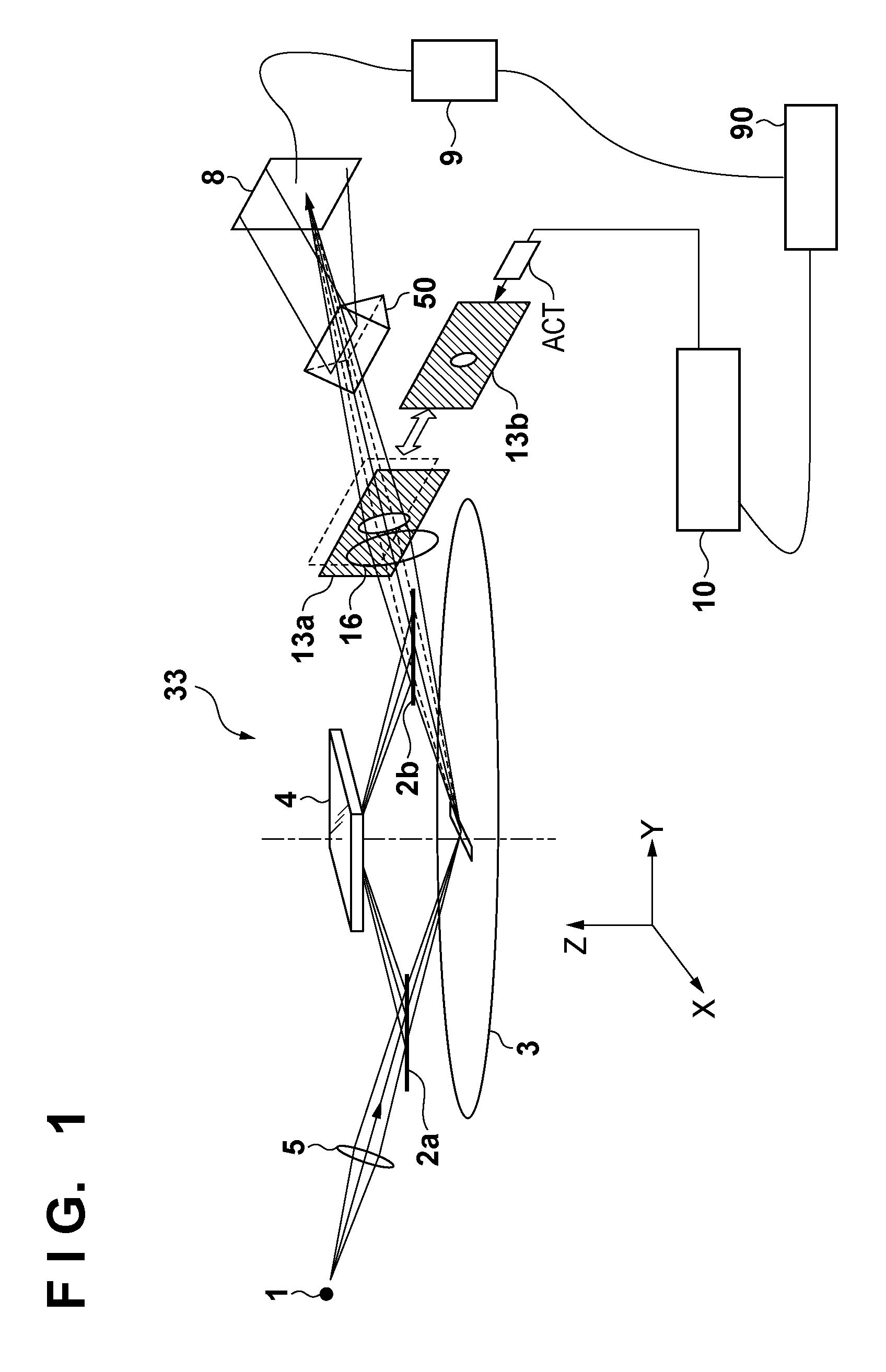
[0028]FIG. 1 is a view showing the schematic configuration of a measurement apparatus 33 according to the present invention. The measurement apparatus 33 is configured to detect the surface position of a substrate (for example, a wafer) 3 as an object to be measured, that is, the position of the surface of the substrate 3 in the height direction (Z-direction) as the physical information of the substrate 3 while scanning the substrate 3 in one direction (Y-direction), thereby measuring the surface shape of the substrate 3. Note that the measurement apparatus 33 also serves as a measurement apparatus which measures the surface position (level) of the object to be measured as the physical information of the substrate 3. The measurement apparatus 33 includes a light source 1, beam splitter 2a, reference surface 4, beam combiner 2b, imaging optical systems 5 and 16, aperture stops 13a and 13b, spectrometer 50, image sensor 8, calculating unit 9, coherence controller 10, and main controll...
second embodiment
[0056]At an entrance end 28a of the bundled fiber 28, fiber wires are bundled in a nearly circular shape, as shown in FIG. 9, so light can be efficiently received from the light source 1. On the other hand, at an exit end 28b of the bundled fiber 28, fiber wires are bundled in a rectangular shape. This makes it possible to freely arrange the light source 1 at a position spaced apart from the imaging optical system 24, thereby reducing the adverse thermal effect that the light source 1 exerts on the imaging optical system 24. Further, varying the array of wires of the bundled fiber 28 in the interval from the entrance end 28a to the exit end 28b provides the same function as that of the transmissive slit plate 30 described in the The imaging optical system 24 can be implemented as, for example, an enlargement optical system, and guide measurement light onto the substrate 3 in a wide range in the X-direction.
[0057]Sets of fiber wires of an entrance end 29a and exit end 29b of the bun...
fifth embodiment
[0064]An exposure apparatus EX according to the present invention will be described below with reference to FIG. 12. The above-mentioned measurement apparatus 33 is built into the exposure apparatus EX. The exposure apparatus EX includes, for example, an illumination system IL, original stage mechanism RSM, projection optical system 32, substrate stage mechanism WSM, and controller 1000. The controller 1000 controls the illumination system IL, original stage mechanism RSM, projection optical system 32, substrate stage mechanism WSM, and measurement apparatus 33. The final surface (flat surface) of the projection optical system 32 can be used as a reference surface 4 of the measurement apparatus 33. The illumination system IL includes a light source unit 800 and an illumination optical system 801 which illuminates an original (reticle) 31 with light supplied from the light source unit 800. The light source unit 800 can be, for example, a laser. The laser can be an ArF excimer laser w...
PUM
 Abstract
Description
Claims
Application Information