Simultaneous Sensing of Multiple Wordlines and Detection of NAND Failures

a technology of simultaneous sensing and wordlines, applied in static storage, digital storage, instruments, etc., can solve problems such as mechanical failure, bulky disk drives, and unsuitable mobile and handheld environments, and achieve the effect of avoiding mechanical failure, avoiding mechanical failure, and avoiding mechanical failur

Active Publication Date: 2013-01-31
SANDISK TECH LLC
View PDF5 Cites 112 Cited by
  • Summary
  • Abstract
  • Description
  • Claims
  • Application Information

AI Technical Summary

Benefits of technology

[0018]In a first set of aspects, a method of operating a memory device including a plurality of memory cells formed along word lines and bit lines is presented. The method includes performing a write operation, including the programming of a plurality of memory cells along a corresponding plurality of selected word lines and one or more selected bit lines, and subsequently performing a composite sensing operation. The composite sensing operation includes: concurrently applying a plurality of first sensing voltages to distinguish between levels of programming to the corresponding plurality of selected word lines; and concurrently performing, for each of the one or more selected bit lines, a first combined sensing operation of the corresponding plurality of memory cells along the plurality of selected word lines while the plurality of first sensing voltages are applied to them. The result of the first combined sensing operation is dependent upon the state of the plurality of memory cells along the selected bit line.

Problems solved by technology

Conventional mass storage, based on rotating magnetic medium such as hard drives and floppy disks, is unsuitable for the mobile and handheld environment.
This is because disk drives tend to be bulky, are prone to mechanical failure and have high latency and high power requirements.
These undesirable attributes make disk-based storage impractical in most mobile and portable applications.
Obviously, the more bits a memory cell is configured to store, the smaller is the margin of error it has to operate in.
Both techniques require the memory to operate with increasing tighter margin of error.
The more bits it has to correct, the more complex and computationally intensive will the ECC be.
As the flash memory ages, its error rate increases rapidly near the end of life of the device.
Using ECC to correct a worst-case number of error bits will consume a great amount processing time.
The more bits it has to correct, the more computational time is required.
Such dedicated hardware can take up a considerable amount of space on the controller ASIC chip.
Moreover, for most of the life time of the device, the ECC is only marginally utilized, resulting in its large overheads being wasted and realizing no real benefits.

Method used


Image

  • Simultaneous Sensing of Multiple Wordlines and Detection of NAND Failures
  • Simultaneous Sensing of Multiple Wordlines and Detection of NAND Failures
  • Simultaneous Sensing of Multiple Wordlines and Detection of NAND Failures

Examples


Embodiment Construction

Memory System

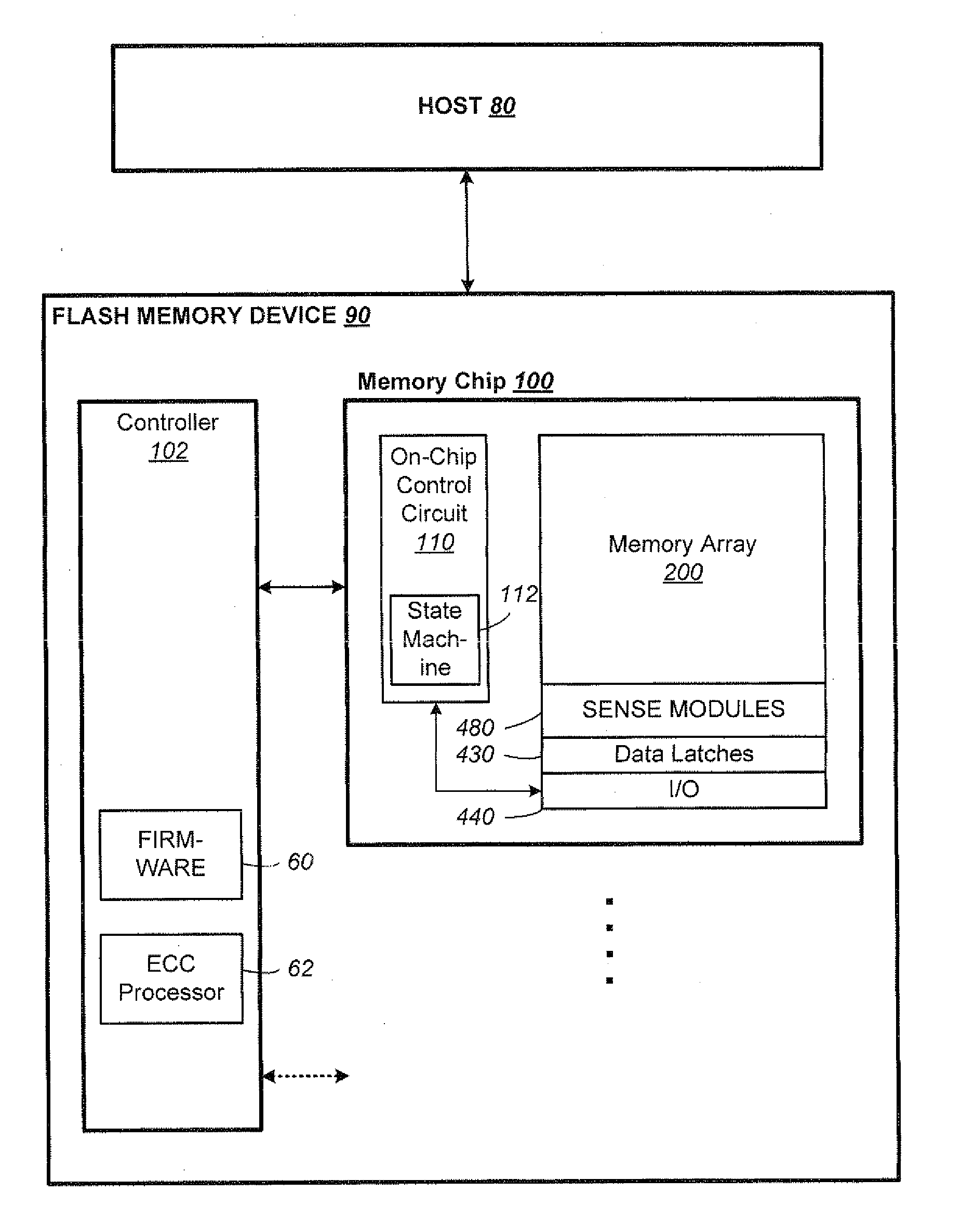
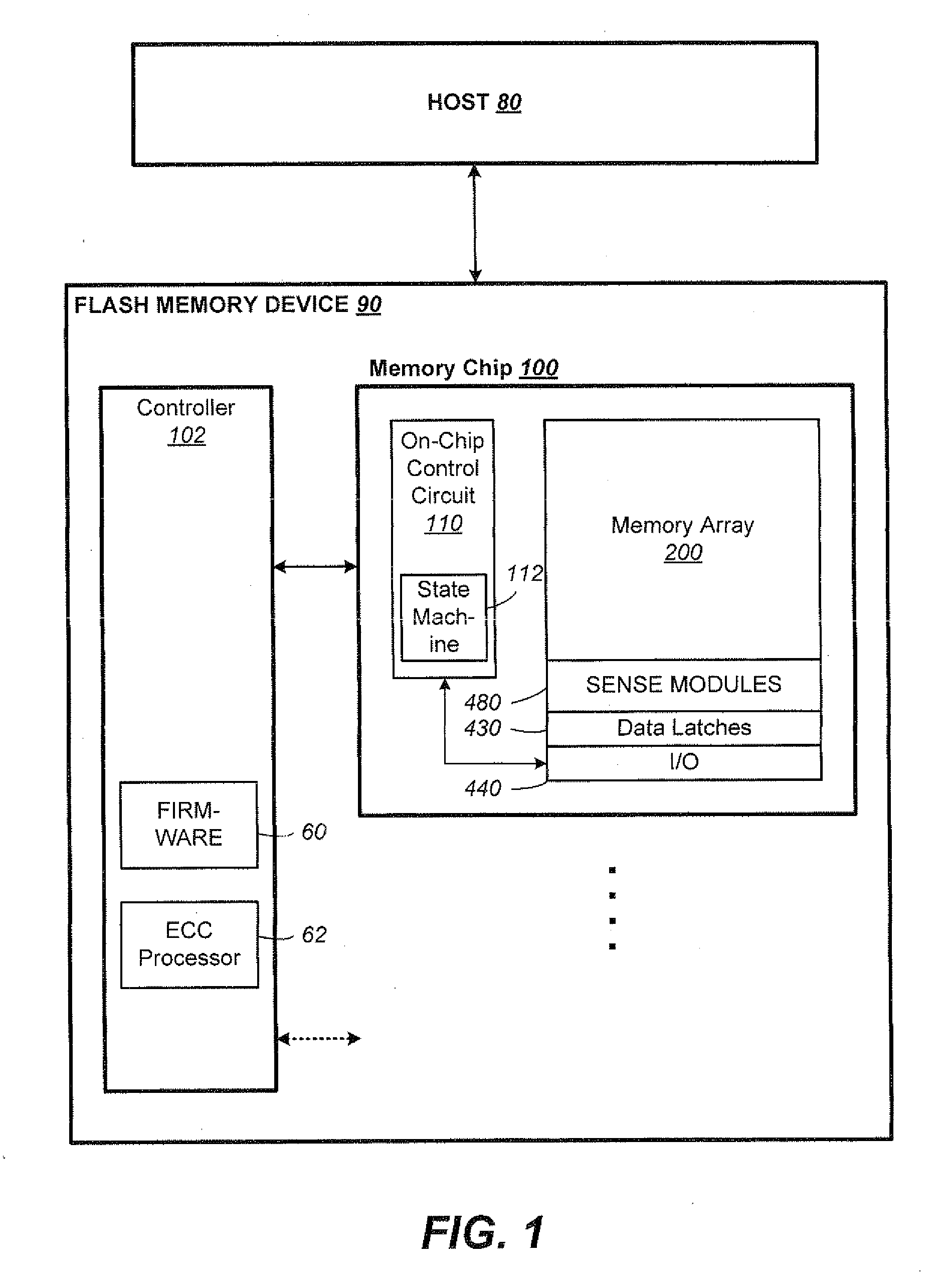
[0070]FIG. 1 illustrates a host in communication with a memory device in which the features of the present invention are embodied. The host 80 typically sends data to be stored at the memory device 90 or retrieves data by reading the memory device 90. The memory device 90 includes one or more memory chip 100 managed by a controller 102. The memory chip 100 includes a memory array 200 of memory cells with each cell capable of being configured as a multi-level cell (“MLC”) for storing multiple bits of data. The memory chip also includes peripheral circuits such as sense modules 480, data latches 430 and I / O circuits 440. An on-chip control circuitry 110 controls low-level memory operations of each chip. The control circuitry 110 is an on-chip controller that cooperates with the peripheral circuits to perform memory operations on the memory array 200. The control circuitry 110 typically includes a state machine 112 to provide chip level control of memory operations.

[0071]I...


PUM


Abstract

Techniques for a post-write read are presented. In an exemplary embodiment, a combined simultaneous sensing of multiple word lines is used in order to identify a problem in one or more of these word lines. That is, sensing voltages are concurrently applied to the control gates of more than one memory cell whose resultant conductance is measured on the same bit line. The combined sensing result is use for measuring certain statistics of the cell voltage distribution (CVD) of multiple word lines and comparing it to the expected value. In case the measured statistics are different than expected, this may indicate that one or more of the sensed word lines may exhibit a failure and more thorough examination of the group of word lines can be performed.

Description

CROSS-REFERENCE TO RELATED APPLICATIONS[0001]This application is a continuation in part of U.S. patent application Ser. No. 13 / 193,083 and U.S. Provisional Patent Application No. 61 / 512,749, both filed Jul. 28, 2011, and is related to U.S. patent application Ser. Nos. 13 / 193,148, also filed Jul. 28, 2011, and 13 / 280,217 filed Oct. 24, 2011, which applications are incorporated herein by this reference in their entirety.BACKGROUND OF THE INVENTION[0002]This application relates to the operation of re-programmable non-volatile memory systems such as semiconductor flash memory, and, more specifically, to handling and efficient managing of errors in memory operations.[0003]Solid-state memory capable of nonvolatile storage of charge, particularly in the form of EEPROM and flash EEPROM packaged as a small form factor card, has recently become the storage of choice in a variety of mobile and handheld devices, notably information appliances and consumer electronics products. Unlike RAM (rando...

Claims


Application Information

Patent Timeline
Patent Type & Authority Applications(United States)
IPC IPC(8): G11C16/10G11C16/04
CPCG11C11/5642G11C2211/5641G11C29/04G11C16/3459G11C29/50004
Inventor SHARON, ERANLI, YANLEE, DANAALROD, IDAN
Owner SANDISK TECH LLC
Why Eureka
Try Eureka