

Semiconductor light emitting element
- Summary
- Abstract
- Description
- Claims
- Application Information
AI Technical Summary
Benefits of technology
Problems solved by technology
Method used
Image

Examples
embodiment 2
[0062]FIG. 7 is a cross-sectional view showing the configuration of a semiconductor light emitting element 2 according to Embodiment 2 of the present invention. In FIG. 7, the part below the light reflecting layer 20 is the same as in the semiconductor light emitting element 1 according to the above embodiment 1 and hence is omitted.
[0063]In the semiconductor light emitting element 2, a semiconductor film 10a is provided with an n-type contact layer 15a of a relatively high carrier concentration and an n-type clad layer 11a of a relatively low carrier concentration on the light-extraction-surface side of a light emitting layer 12a, and a p-type contact layer 14a of a relatively high carrier concentration and a p-type clad layer 13a of a relatively low carrier concentration on the light-reflecting-surface side thereof.
[0064]The n-type contact layer 15a is made of, e.g., GaAs of 10 nm thickness having a carrier concentration of 1×1019 cm−3. The n-type clad layer 11a is formed of, e.g....
embodiment 3
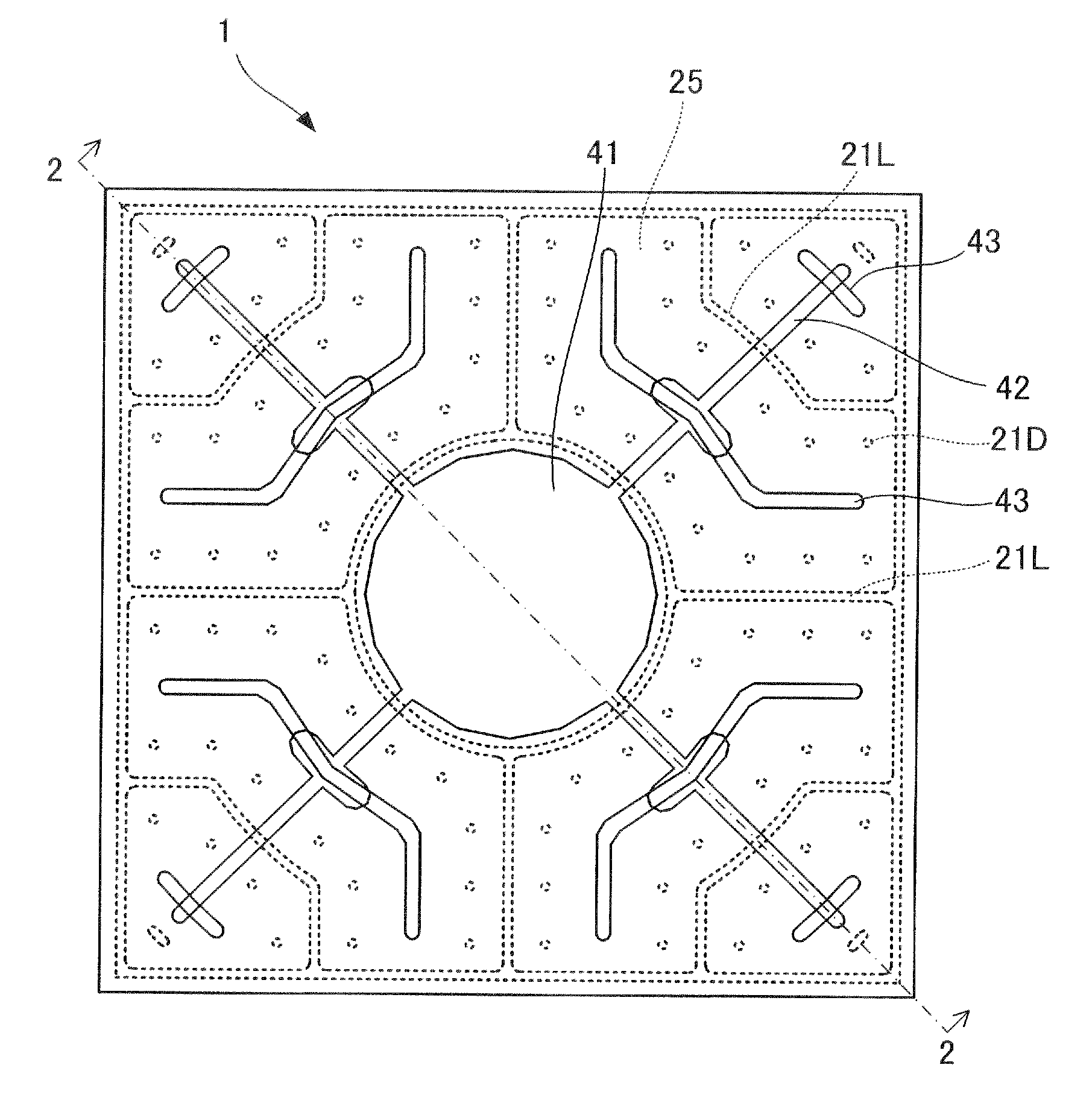
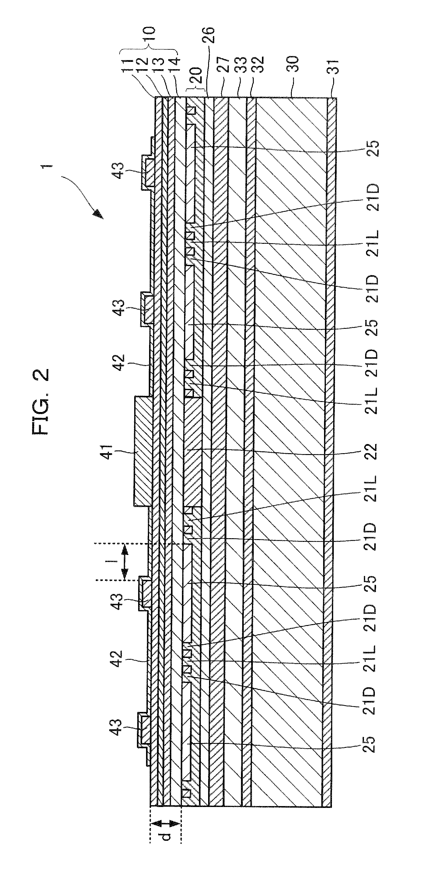
[0072]FIG. 9A is a plan view showing the configuration of a semiconductor light emitting element 3 according to Embodiment 3 of the present invention, and FIG. 9B is a cross-sectional view taken along line 9b-9b in FIG. 9A. In FIG. 9A, a surface electrode provided on the light-extraction-surface side is indicated by solid lines, and a reflecting electrode provided on the light-reflecting-surface side is indicated by broken lines and hatching. The semiconductor light emitting element 3 differs mainly in the material of the semiconductor film and the electrode configuration from the semiconductor light emitting element 1 according to the previously-described embodiment 1. The other configuration is the same as in the semiconductor light emitting element 1 according to the embodiment 1.
[0073]The semiconductor film 10b is constituted by a GaN-based semiconductor and configured with an n-type clad layer 11b, a light emitting layer 12b, and a p-type clad layer 13b that are laid one over a...
embodiment 4
[0082]FIG. 10A is a plan view showing the configuration of a semiconductor light emitting element 4 according to Embodiment 4 of the present invention, and FIG. 10B is a cross-sectional view taken along line 10b-10b in FIG. 10A. In FIG. 10A, a surface electrode provided on the light-extraction-surface side is indicated by solid lines, and a reflecting electrode provided on the light-reflecting-surface side is indicated by broken lines and hatching.
[0083]In the semiconductor light emitting element 4, the semiconductor film 10c is constituted by a GaN-based semiconductor and configured with a damaged layer 16c, an n-type clad layer 11c, a light emitting layer 12c, and a p-type clad layer 13c that are laid one over another in that order from the light-extraction-surface side.
[0084]The damaged layer 16c is constituted by, e.g., GaN of 1 μm thickness. The damaged layer 16c is a layer which is higher in inner defect density than the other layers and thus is of high resistance. The damaged...
PUM
 Abstract
Description
Claims
Application Information