Supercharge Your Innovation With Domain-Expert AI Agents!

Trench-gate metal oxide semiconductor device and fabricating method thereof

a metal oxide semiconductor and trench-gate technology, applied in the direction of semiconductor devices, basic electric elements, electrical appliances, etc., can solve the problems of limited trench-gate metal oxide semiconductor field effect transistor development, the effect of reducing the fabrication cost and reducing the current density of the effect transistor, and the failure of the effect transistor to simultaneously increase the device current density and reduce the on-resistan

Active Publication Date: 2013-02-14
UNITED MICROELECTRONICS CORP
View PDF3 Cites 11 Cited by
  • Summary
  • Abstract
  • Description
  • Claims
  • Application Information

AI Technical Summary

Benefits of technology

The patent text describes a method for making a semiconductor device by integrating two processes: shallow trench isolation and trench etch. This method provides cost savings, higher integration of semiconductor processes, and reduced fabrication costs. In summary, this method allows for more efficient and cost-effective semiconductor device fabrication.

Problems solved by technology

As known, the conventional planar channel field effect transistor fails to simultaneously increase device current density and reduce the on-resistance.
However, since the integrated circuit becomes more and more complicated, the development of the trench-gate metal oxide semiconductor field effect transistor is limited.

Method used


Image

  • Trench-gate metal oxide semiconductor device and fabricating method thereof
  • Trench-gate metal oxide semiconductor device and fabricating method thereof
  • Trench-gate metal oxide semiconductor device and fabricating method thereof

Examples


Embodiment Construction

[0028]The present invention will now be described more specifically with reference to the following embodiments. It is to be noted that the following descriptions of preferred embodiments of this invention are presented herein for purpose of illustration and description only. It is not intended to be exhaustive or to be limited to the precise form disclosed.

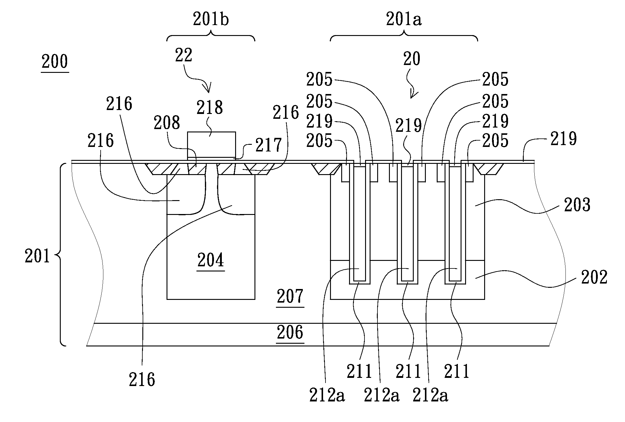
[0029]The present invention provides an improved trench-gate metal oxide semiconductor device and a fabricating method of the trench-gate metal oxide semiconductor device. In accordance with a key feature of the present invention, two metal oxide semiconductor structures with a planar channel and a vertical channel are integrated, so that the fabricating cost is reduced.

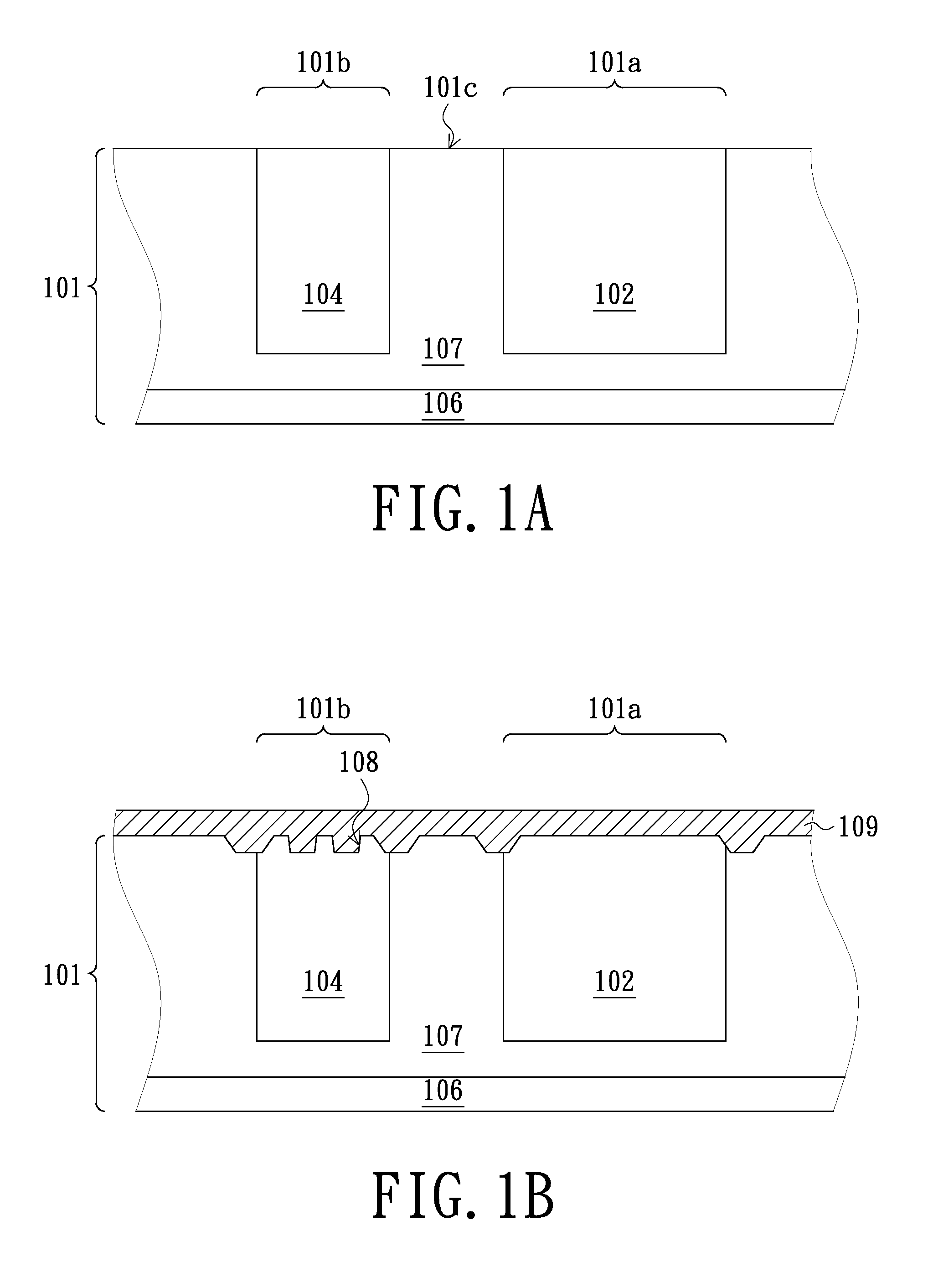
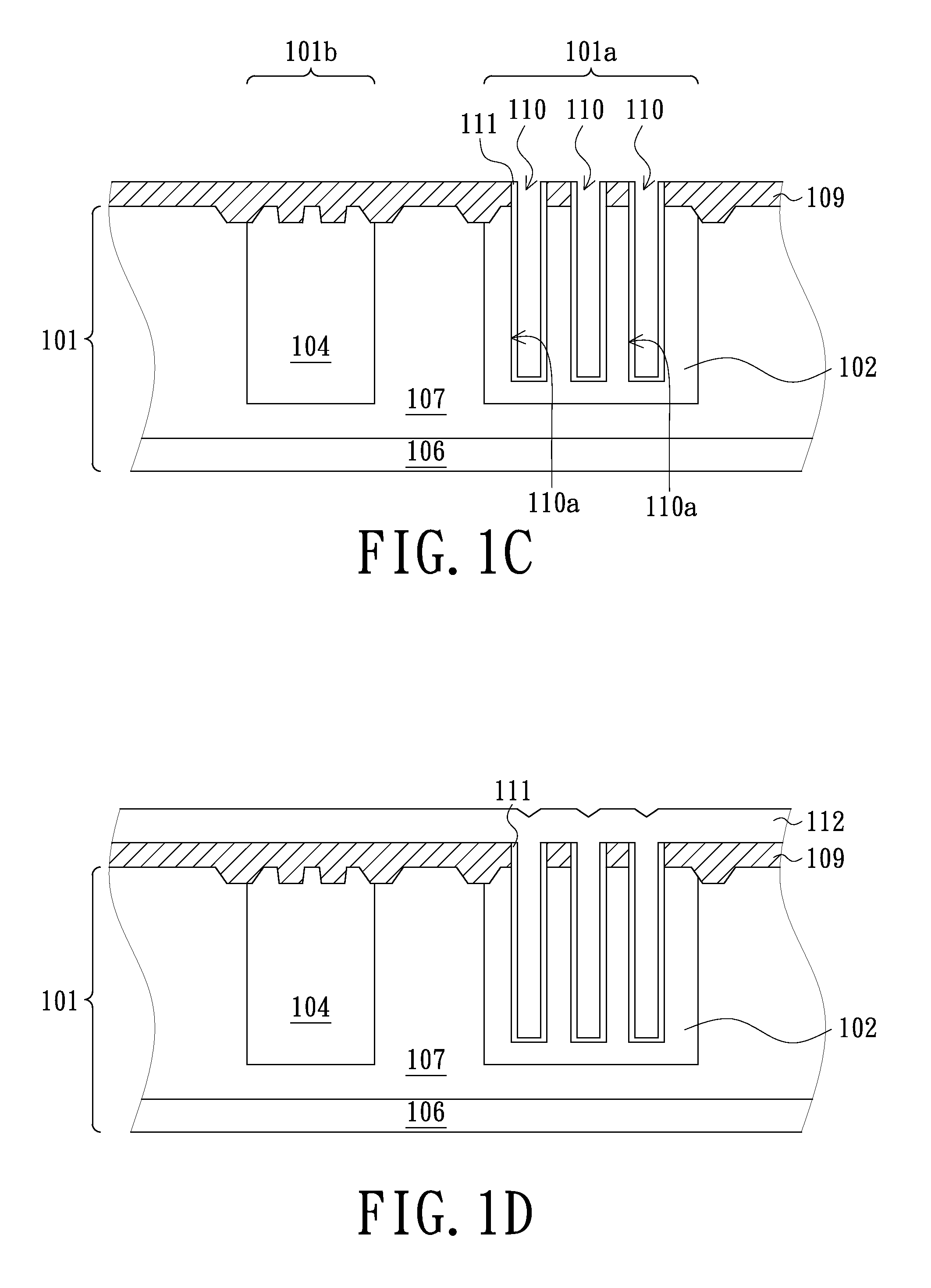
[0030]FIGS. 1A˜1I are schematic cross-sectional views illustrating a method for fabricating a complementary metal-oxide-semiconductor (CMOS) device 100 according to an embodiment of the present invention. The method for fabricating the CMOS device comprises the fo...


PUM


Abstract

A trench-gate metal oxide semiconductor device includes a substrate, a first gate dielectric layer, a first gate electrode and a first source / drain structure. The substrate has a first doping region, a second doping region and at least one trench. A P / N junction is formed between the first doping region and the second doping region. The trench extends from a surface of the substrate to the first doping region through the second doping region and the P / N junction. The first gate dielectric layer is formed on a sidewall of the second trench. The first gate electrode is disposed within the trench. A height difference between the top surface of the first gate electrode and the surface of the substrate is substantially smaller than 1500 Å. The first source / drain structure is formed in the substrate and adjacent to the first gate dielectric layer.

Description

FIELD OF THE INVENTION[0001]The present invention relates to a semiconductor device and a fabricating method thereof, and more particularly to a trench-gate metal oxide semiconductor device and a fabricating method thereof.BACKGROUND OF THE INVENTION[0002]A trench-gate metal oxide semiconductor (TMOS) field effect transistor is a semiconductor device whose gate structure is embedded in the etch trench of the epitaxial layer. Since the carrier drift path of such field effect transistor is formed along the sidewall of the trench, the channel length of the field effect transistor can be largely increased and the resistance of the characteristic channel can be largely reduced by about 30%. Therefore, if the operating current is constant, the static power loss is reduced and the device current density is increased. As known, the conventional planar channel field effect transistor fails to simultaneously increase device current density and reduce the on-resistance. However, the trench-gat...

Claims


Application Information

Patent Timeline
IPC IPC(8): H01L29/78H01L21/336
CPCH01L29/6634H01L29/7397H01L2924/10253H01L29/7835H01L29/7813H01L29/66666H01L29/4236H01L29/7827H01L21/823885H01L27/0922H01L2924/00
Inventor LIU, KUAN-LINGUENG, SHIH-YUAN
Owner UNITED MICROELECTRONICS CORP
Features
  • R&D
  • Intellectual Property
  • Life Sciences
  • Materials
  • Tech Scout
  • Unparalleled Data Quality
  • Higher Quality Content
  • 60% Fewer Hallucinations
Learn More