Wire-grid polarizer and process for producing the same
a polarizer and wire-grid technology, applied in the direction of polarising elements, instruments, optics, etc., can solve the problems of low productivity of the wire-grid polarizer in item (1), low light use efficiency of the absorption polarizer, etc., and achieve low angle dependency, low wavelength dependency, and high degree of polarization
- Summary
- Abstract
- Description
- Claims
- Application Information
AI Technical Summary
Benefits of technology
Problems solved by technology
Method used
Image
Examples
first embodiment
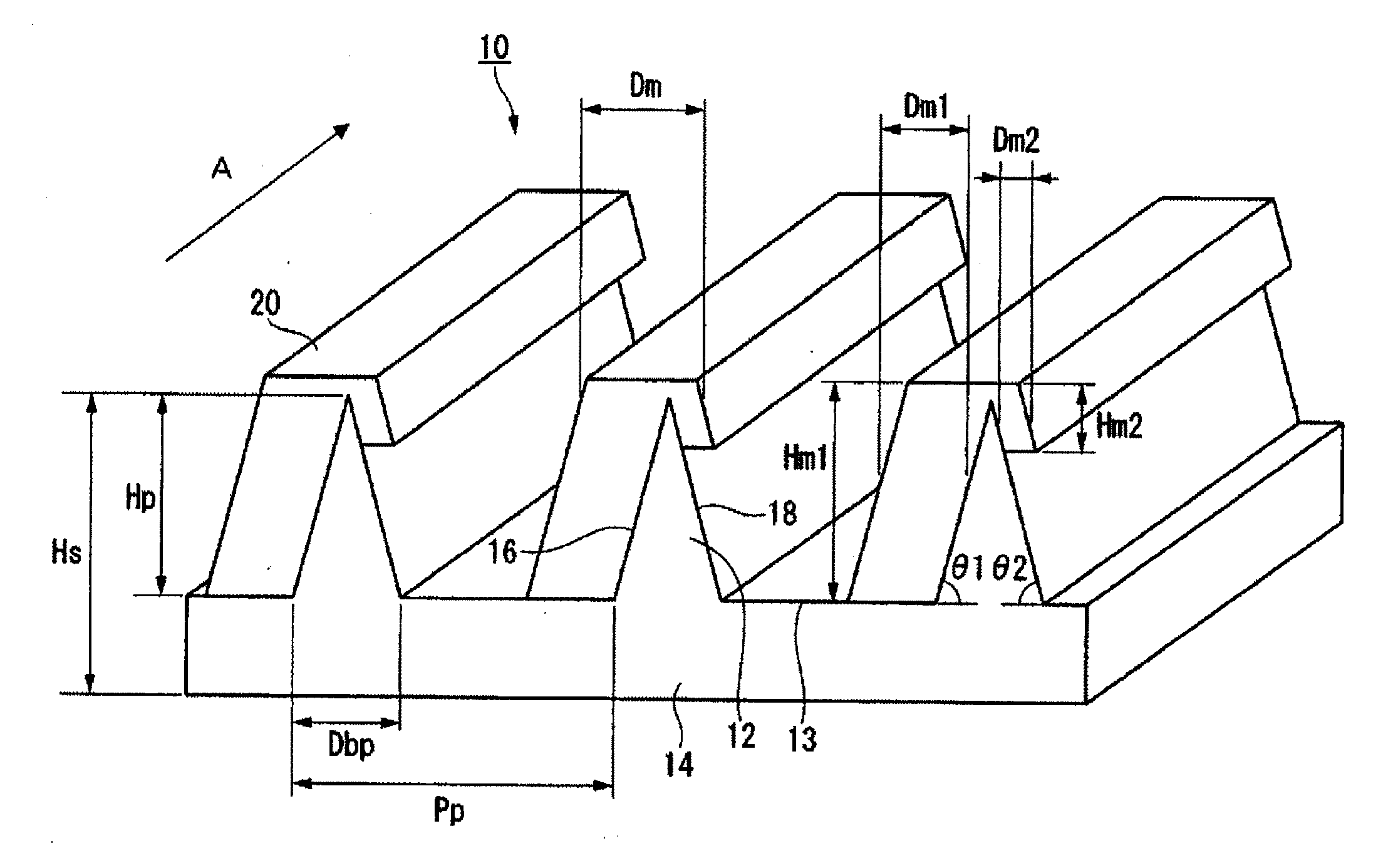
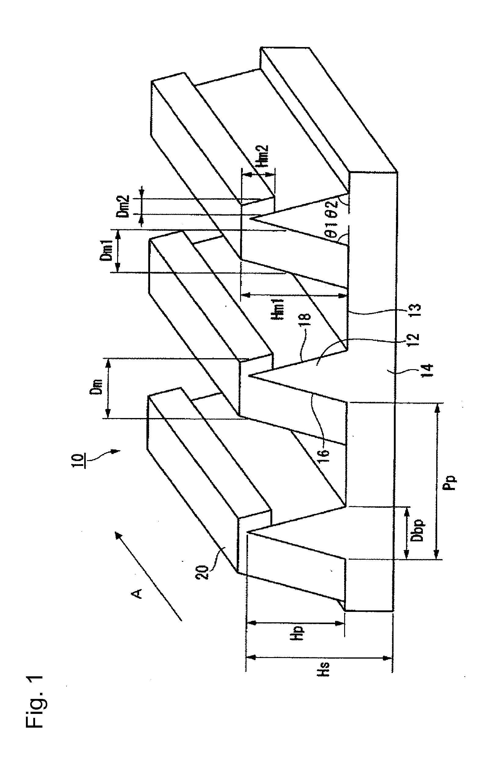
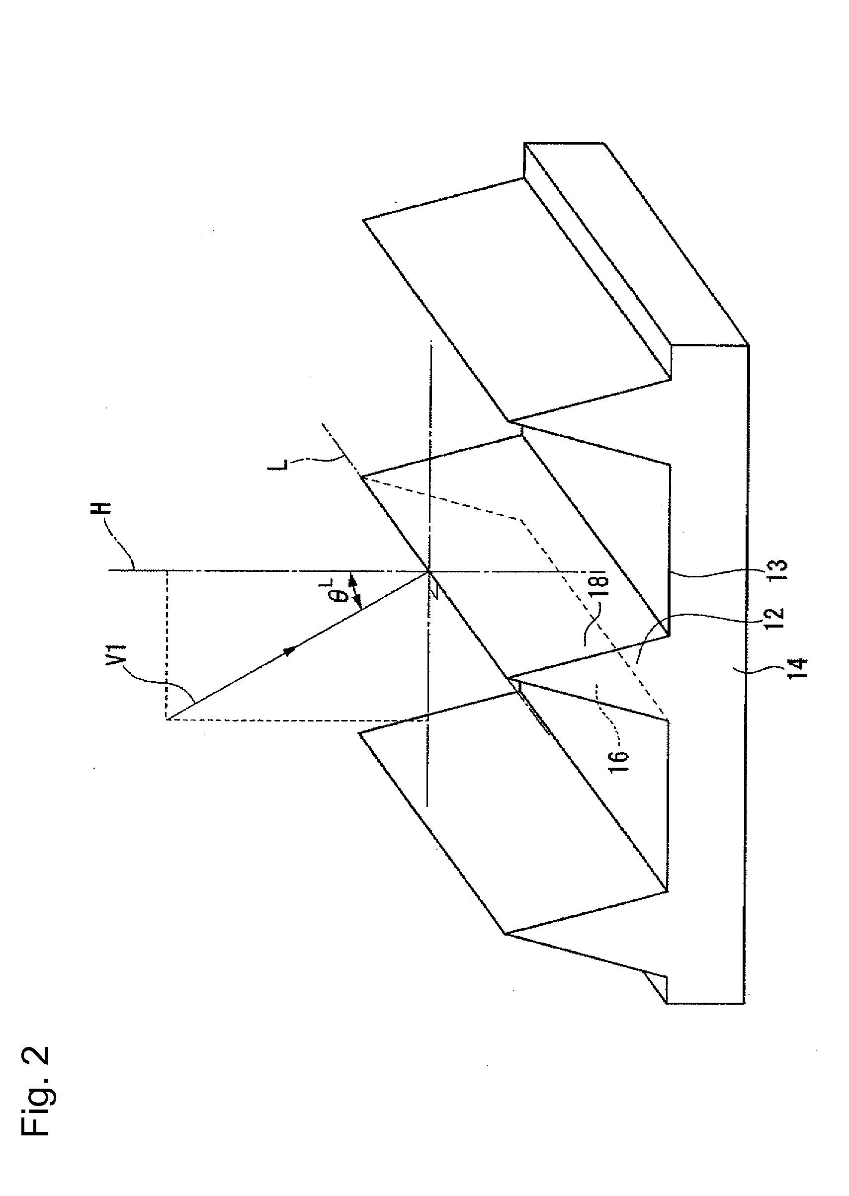
[0081]FIG. 1 is a perspective view showing the wire-grid polarizer according to a first embodiment of the present invention. The wire-grid polarizer 10 includes a light-transmitting substrate 14 having a plurality of ridges 12 formed in parallel to one another at certain pitches Pp through respective flat portions 13 disposed between adjacent ridges 12, each of the ridges extending in an direction indicated by an arrow A and having a triangular cross section; and a metal layer 20 composed of metal or a metal compound, the metal layer covering the entirety of a first lateral face 16 of each ridge 12, a part of the flat portion 13 adjacent to the first lateral face 16, between adjacent ridges 12, and a part of a second lateral face 18 of each ridge 12 adjacent to the first lateral face 16 such that the remaining part of the flat portion 13 and the remaining part of the second lateral face 18 are covered with no metal layer. The metal layer 20 extends in the longitudinal direction of e...
second embodiment
[0113]FIG. 3 is a perspective view showing the wire-grid polarizer according to a second embodiment of the present invention. The wire-grid polarizer 10 includes a light-transmitting substrate 14 having a plurality of ridges 12 formed in parallel to one another at certain pitches Pp through the flat portions 13 on the respective grooves disposed between adjacent ridges 12, each of the ridges having a trapezoidal cross section; and a metal layer 20 composed of metal or a metal compound, the metal layer covering the entirety of a first lateral face 16 of each ridge 12, a part of the flat portion 13 adjacent to the first lateral face 16, between adjacent ridges 12, the entirety of a top portion 19 of each ridge 12 adjacent to the first lateral face 16, and a part of a second lateral face 18 of each ridge 12 adjacent to the top portion 19 such that the remaining part of the flat portion 13 and the remaining part of the second lateral portion 18 are covered with no metal layer. The metal...
example 1
Preparation of Light-Transmitting Substrate
[0134]A photocurable composition 1 was applied by a spin coating method on the surface of a highly transmitting polyethylene terephthalate (PET) film (manufactured by Teijin DuPont Films Japan Limited, Teijin Tetoron O3, 100 mm×100 mm) having a thickness of 100 μm to form a coating film of the photocurable composition 1 having a thickness of 5 μm.
[0135]A quartz mold, which had a plurality of grooves formed at certain pitches so as to extend in parallel to one another through the respective flat portions between adjacent grooves (area: 150 mm×150 mm, pattern area: 100 mm×100 mm, groove pitch Pp: 160 nm, groove width Dbp: 65 nm, groove depth Hp: 200 nm, groove length: 100 mm, cross-sectional shape of groove: substantially isosceles triangle), was pressed against the coating film of the photocurable composition 1 with 0.5 MPa (gauge pressure) and at 25° C. so as to be brought into contact with the coating film of the photocurable composition 1...
PUM
 Abstract
Description
Claims
Application Information


