Method for Determining BSIMSOI4 DC Model Parameters

Active Publication Date: 2013-02-28
SHANGHAI INST OF MICROSYSTEM & INFORMATION TECH CHINESE ACAD OF SCI
View PDF13 Cites 7 Cited by
  • Summary
  • Abstract
  • Description
  • Claims
  • Application Information

AI Technical Summary

Benefits of technology

[0030]In the present invention, in the condition of different temperatures and different bias voltages, electrical performance of SOI MOSFET devices of various sizes, including MOSFET devices of a body leading-out structure and MOSFET devices of a floating structure, is tested, proper test curves are successively selected according to model equations, and various kinds of parameters are successively determined, thereby accurately and effectively extracting DC parameters of the BSIMSOI4 model.
[0031]In the present invention, a body area of the SOI MOSFET is independently and specifically modeled by using test data of the device of a body leading-out structure and the device of a floating structure, and model parameters are extracted based on a property curve without a self-heating effect, so as to conform to actual conditions of the devices. In addition, since t

Problems solved by technology

Due to a complicated physical mechanism in the SOI MOSFET device, the SOI MOSFET device h

Method used


Image

  • Method for Determining BSIMSOI4 DC Model Parameters
  • Method for Determining BSIMSOI4 DC Model Parameters
  • Method for Determining BSIMSOI4 DC Model Parameters

Examples


Embodiment Construction

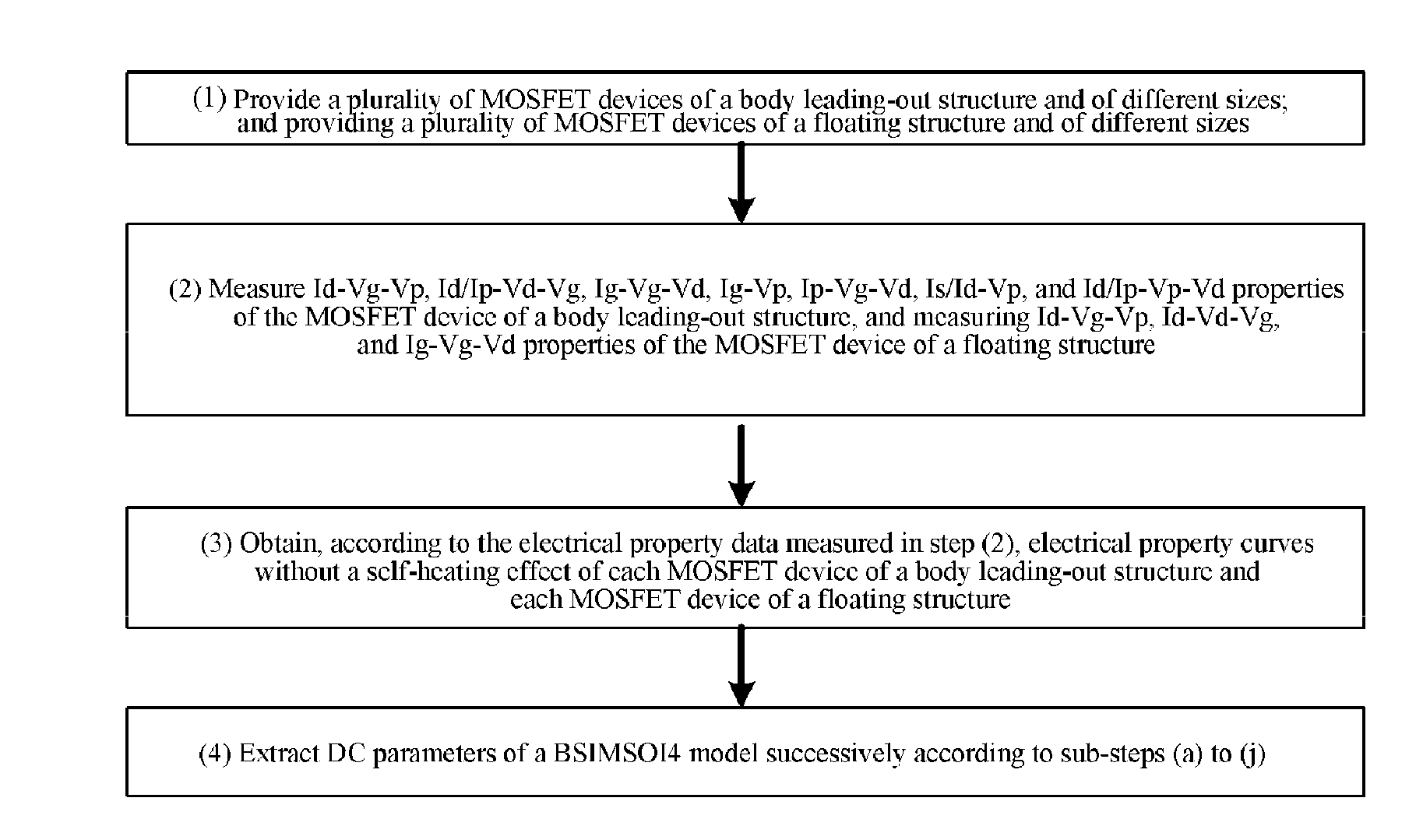
[0037]A device structure of the present invention is further described in the following with reference to the accompanying drawings, and the accompanying drawings are not drawn to scale for ease of showing.

[0038]In this embodiment, taking an SOI MOSFET device model fabricated in a 0.13 μm fabrication process (a designed value of a minimum channel width among the MOSFET devices is 0.13 μm) as an example, a method for determining BSIMSOI4 DC model parameters is provided. Referring to FIG. 4, the method includes the following steps.

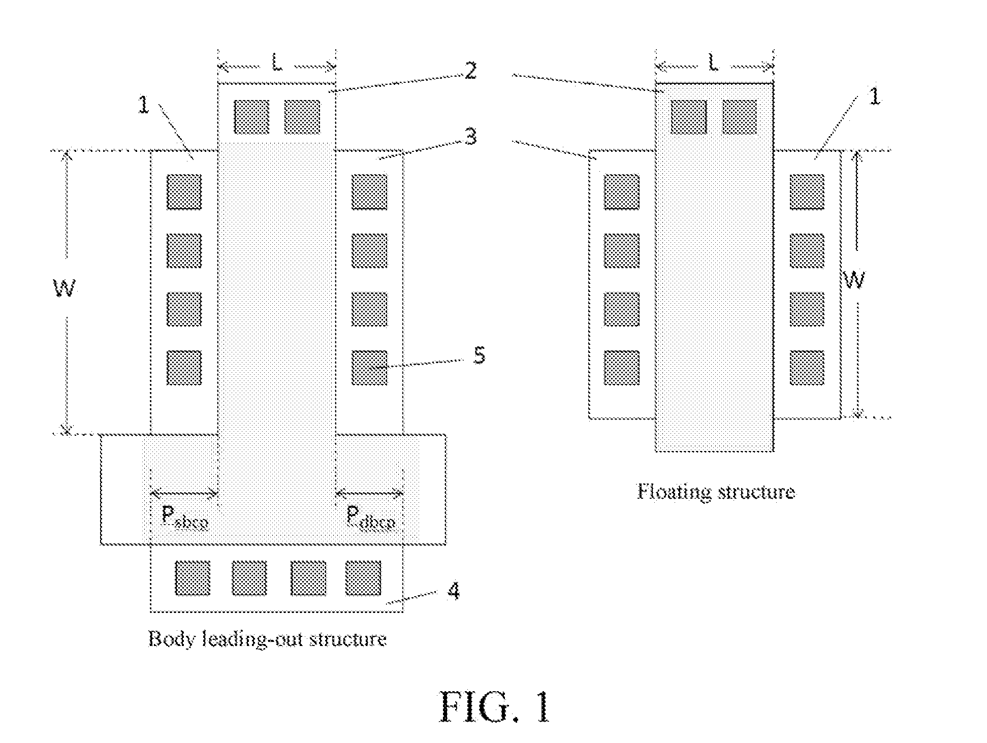
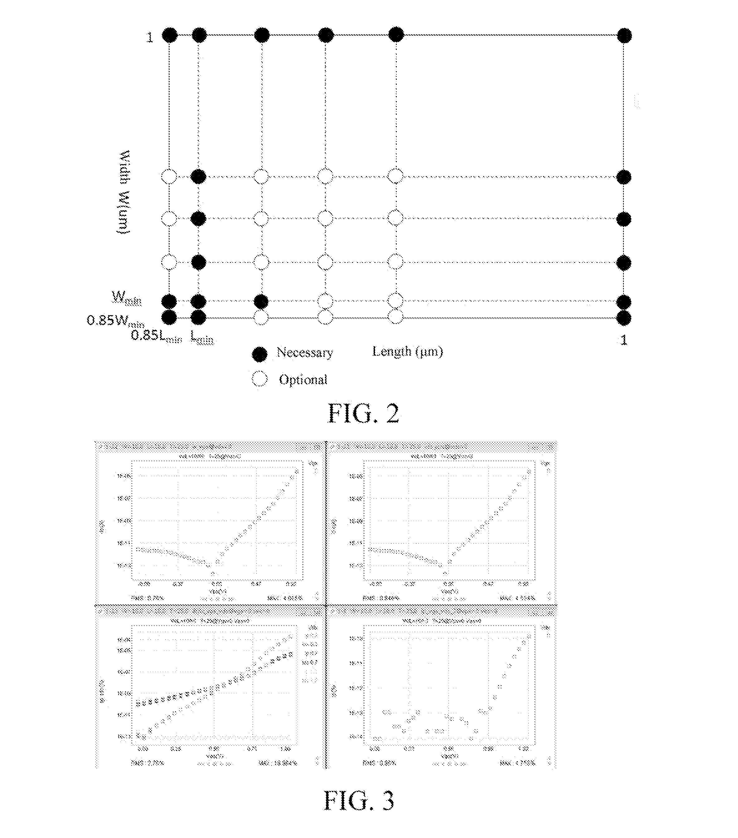
[0039](1) A plurality of MOSFET devices of a body leading-out structure and with different channel lengths L and different channel widths W, and a plurality of MOSFET devices of a floating structure and with different channel lengths L and different channel widths W are provided, where 0.85Lmin≦W≦1 μm, 0.85Lmin≦L≦1 μm, Wmin and Lmin are minimum values determined by a process, and a preferable range of the device sizes is shown in FIG. 2. FIG. 1 shows structu...


PUM


Abstract

The present invention provides a method for determining BSIMSOI4 Direct Current (DC) model parameters, where a plurality of Metal Oxide Semiconductor Field Effect Transistor (MOSFET) devices of a body leading-out structure and of different sizes, and a plurality of MOSFET devices of a floating structure and of different sizes are provided; Id-Vg-Vp, Id/Ip-Vd-Vg, Ig-Vg-Vd, Ig-Vp, Ip-Vg-vd, Is/Id-Vp, and Id/Ip-Vp-Vd properties of all the MOSFET devices of a body leading-out structure, and Id-Vg-Vp, Id-Vd-Vg, and Ig-Vg-Vd properties of all the MOSFET devices of a floating structure are measured; electrical property curves without a self-heating effect of each MOSFET device of a body leading-out structure and each MOSFET device of a floating structure are obtained; and then DC parameters of a BSIMSOI4 model are successively extracted according to specific steps. In the present invention, proper test curves are successively selected according to model equations, and various kinds of parameters are successively determined, thereby accurately and effectively extracting the DC parameters of the BSIMSOI4 model.

Description

BACKGROUND OF THE PRESENT INVENTION[0001]1. Field of Invention[0002]The present invention relates to a method for determining model parameters of a Silicon On Insulator (SOI) Metal Oxide Semiconductor Field Effect Transistor (MOSFET) device, and particularly to a method for determining BSIMSOI4 Direct Current (DC) model parameters, belonging to the field of micro-electronic device modeling.[0003]2. Description of Related Arts[0004]An MOSFET is a four-port semiconductor device, where different excitation is applied to each port, and a drain current of the device also changes accordingly. An input / output mathematical expression is obtained by establishing a mathematical model of the device, and circuit designers use the model to perform SPICE emulation of circuit design. Currently, multiple kinds of mathematical models with respect to the MOSFET are proposed, and each kind of model includes a large number of parameters. A BSIM model is a standard of a device model, and is widely used ...

Claims


Application Information

Patent Timeline
IPC IPC(8): G06F17/10
CPCG06F17/5036G01R31/2628G06F30/367G01R31/2603
Inventor CHEN, JINGWU, QINGQINGLUO, JIEXINCHAI, ZHANWANG, XI
Owner SHANGHAI INST OF MICROSYSTEM & INFORMATION TECH CHINESE ACAD OF SCI
Why Eureka
Try Eureka