Abnormality detecting unit and abnormality detecting method

a detection unit and abnormality technology, applied in the direction of individual semiconductor device testing, electric discharge tubes, instruments, etc., can solve the problems of long waiting time between the wafer process and the test process, abnormal electric discharge such as arc discharge, etc., to improve the detection accuracy of abnormal electric discharg

Inactive Publication Date: 2013-03-07
TOKYO ELECTRON LTD
View PDF3 Cites 12 Cited by
  • Summary
  • Abstract
  • Description
  • Claims
  • Application Information

AI Technical Summary

Benefits of technology

[0026]In accordance with the illustrative embodiments, it is possible to provide an abnormality detecting unit and an abnormality detecting method capable of improving detection accuracy of the abnormal electric discharge.

Problems solved by technology

In the processing chamber in which the plasma is generated, a high frequency electric field is concentrated by various factors and an abnormal electric discharge such as an arc discharge may occur.
The abnormal electric discharge may cause an electric discharge mark on a surface of the processing target object or may burn components provided within the processing chamber.
Further, the abnormal electric discharge may peel off reaction products adhering to the components provided within the processing chamber, so that particles may be generated.
However, according to this method, there is a long waiting time between the wafer process and the test process.
Thus, even if any defect of the wafer is detected during the test process, it takes a certain amount of time to stop the operation of the plasma processing apparatus in which the abnormal electric discharge occurs.
Therefore, lots of wafer products are processed in the meantime and lots of inferior chips may be fabricated.
However, since the AE sensor is highly sensitive, the AE signal detected by the AE sensor may contain a noise such as a mechanical vibration caused by opening / closing transfer gate valve and vertically moving a transfer pin in the plasma processing apparatus as well as the signal caused by the plasma abnormal electric discharge.
Therefore, the noise contained in the AE signal may cause a decrease in detection accuracy of the abnormal electric discharge in the plasma processing apparatus.

Method used


Image

  • Abnormality detecting unit and abnormality detecting method
  • Abnormality detecting unit and abnormality detecting method
  • Abnormality detecting unit and abnormality detecting method

Examples


modification example

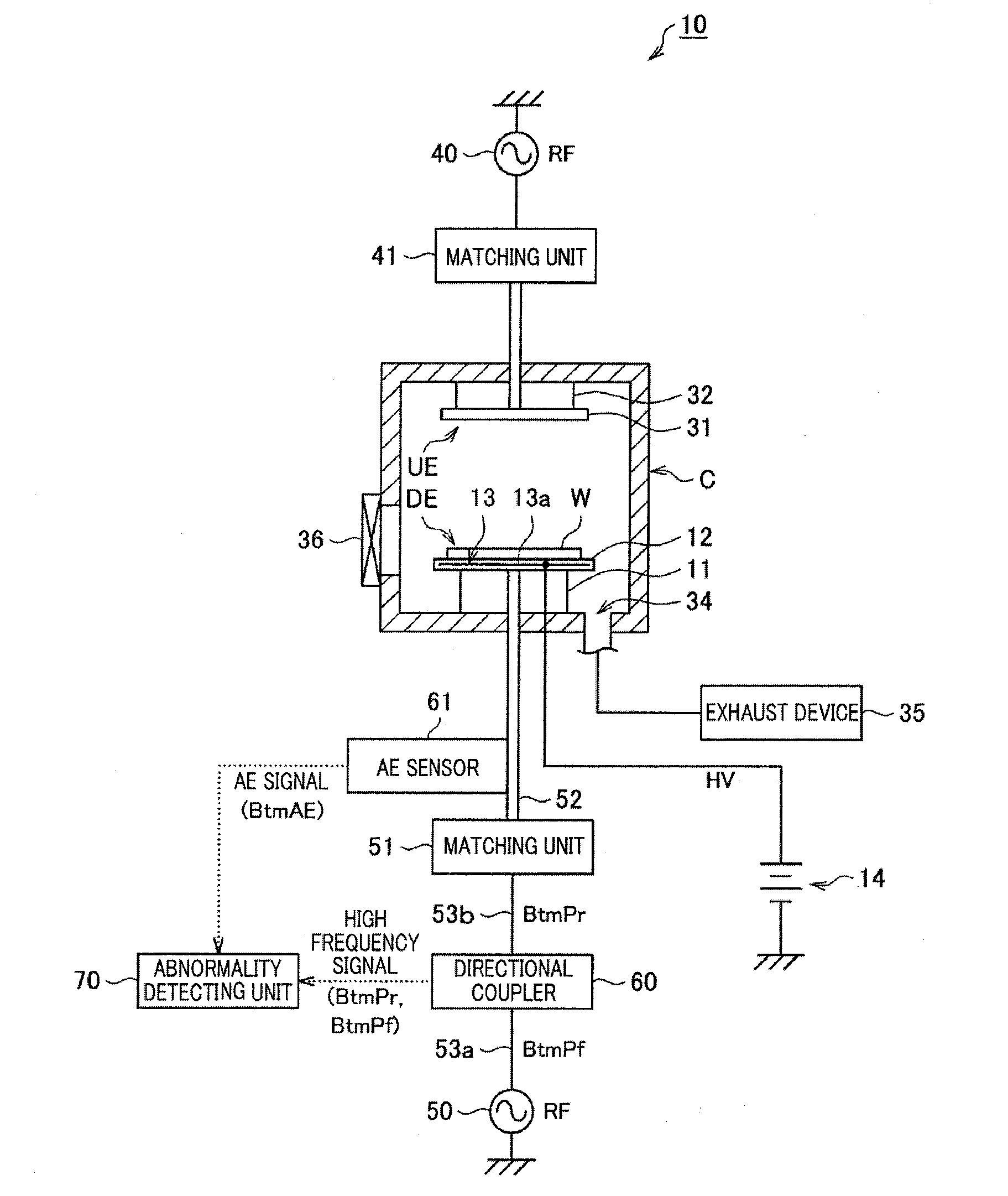
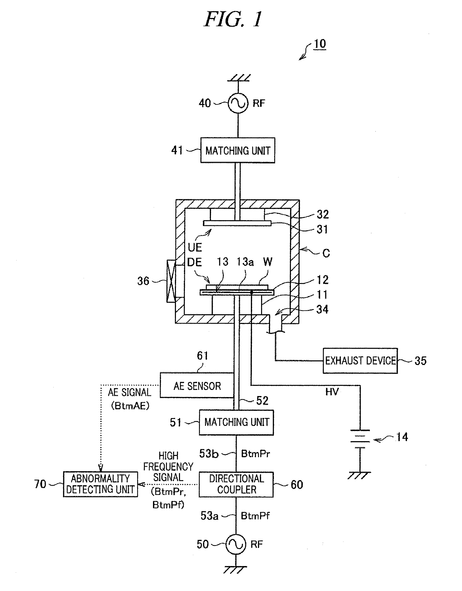
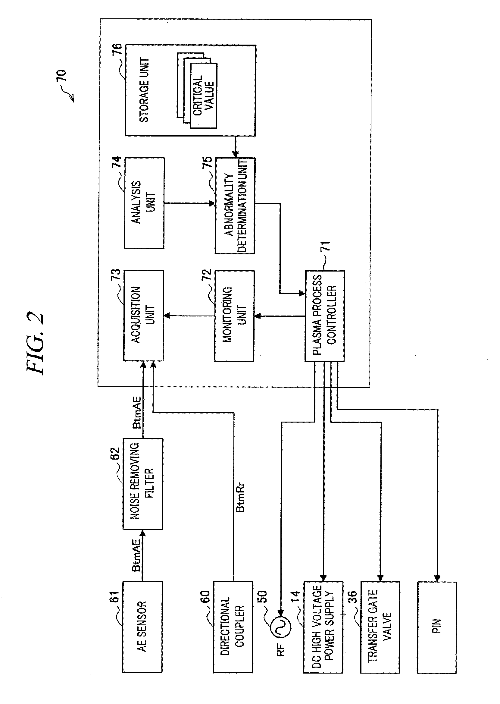
[0107]The abnormal electric discharge detecting operation of the abnormality detecting unit 70 in accordance with a modification example of the illustrative embodiment will be explained with reference to FIG. 14. FIG. 14 is a flow chart showing an abnormality detecting process performed in the abnormality detecting unit 70 in accordance with the modification example of the illustrative embodiment.

[0108]In the abnormality detecting process in accordance with the modification example, the analysis unit 74 acquires sampled data acquired by the acquisition unit 73 during the wafer deviation (step S505). Then, the abnormality determination unit 75 determines whether or not there is an abnormal peak having a value greater than the predetermined critical value C (see FIG. 7) among the sampled data of high frequency signal (step S510). If there is an abnormal peak, the abnormality determination unit 75 determines that there is an abnormal electric discharge on the wafer W (step S515) and in...


PUM

PropertyMeasurementUnit
frequencyaaaaaaaaaa
frequencyaaaaaaaaaa
frequencyaaaaaaaaaa

Abstract

An abnormality detecting unit includes a monitoring unit for monitoring an operation from a wafer deviation starting point to a transfer gate valve opening point after performing a plasma process on the wafer and specifying the operation as a wafer deviation operation; an acquisition unit for acquiring a high frequency signal of at least one of a progressive wave and a reflection wave outputted from a directional coupler between a high frequency power supply for applying a high frequency power into a processing chamber and a matching unit or between a lower electrode as a mounting table for mounting thereon the wafer and the matching unit during the wafer deviation operation; an analysis unit for analyzing a waveform pattern of the high frequency signal; and an abnormality determination unit for determining whether there is an abnormal electric discharge based on an analysis result of the waveform pattern.

Description

CROSS-REFERENCE TO RELATED APPLICATION[0001]This application claims the benefit of Japanese Patent Application Nos. 2011-141492 and 2012-142092 filed on Jun. 27, 2011, and Jun. 25, 2012, respectively, and U.S. Provisional Application Ser. No. 61 / 507,619 filed on Jul. 14, 2011, the entire disclosures of which are incorporated herein by reference.FIELD OF THE INVENTION[0002]The present disclosure relates an abnormality detecting unit and an abnormality detecting method for detecting an abnormal electric discharge in a plasma processing apparatus.BACKGROUND OF THE INVENTION[0003]When performing a process on a processing target object such as a semiconductor wafer (hereinafter, referred to as “wafer”) or a substrate with plasma, a gas is introduced into a processing chamber in which a plasma process is performed and to which a high frequency power is applied. Then, the introduced gas is decomposed to generate plasma. The processing target object is processed with the generated plasma.[0...

Claims


Application Information

Patent Timeline
Patent Type & Authority Applications(United States)
IPC IPC(8): G01R31/26C23F1/08
CPCH01L21/67288H01J37/32944
Inventor NAKAYA, MICHIKOOMINE, HARUKITSUNAMOTO, TETSUNAGAIKE, HIROSHI
Owner TOKYO ELECTRON LTD
Why Eureka
Try Eureka