Method and apparatus for wafer temperature measurement using an independent light source

a technology of independent light source and temperature measurement method, which is applied in the direction of optical radiation measurement, semiconductor/solid-state device testing/measurement, instruments, etc., can solve the problems of affecting device performance, substrate film material damage, and difficulty in determining the overall temperature variation across the substrate surfa

Inactive Publication Date: 2013-03-07
APPLIED MATERIALS INC
View PDF1 Cites 7 Cited by
  • Summary
  • Abstract
  • Description
  • Claims
  • Application Information

AI Technical Summary

Benefits of technology

[0013]Other embodiments provide a method of measuring a substrate temperature during an etching process comprising: providing a substrate in a process chamber at a starting temperature less than a transition point in transmittance for a first infrared wavelength; heating the substrate using radiant energy; pulsing a first light having a wavelength approximately equal to the first infrared wavelength; determining a metric indicative of total transmittance through the substrate when the first light is pulsed on; determining a metric indicative of background transmittance through the substrate when the first light is pulsed off; and determining a process temperature of the substrate based on transmittance of the first infrared wavelength from the first light through the substrate. The first light may be a laser.
[0014]The method may further comprise isolating a metric indicative of transmittance through the substrate from the laser without the background transmittance. Or, the method may further comprise: subtracting (a) the metric indicative of background transmittance through the substrate when the first light is pulsed off from (b) the metric indicative of total transmittance through the substrate when the first light is pulsed on. The wavelength of the infrared laser light can be 1200 nm, and the heating step can further comprise powering on one or more heating lamps. The metric of transmittance can be either a normalized transmission ratio or a light signal measured in voltage.
[0015]In another embodiment, the method may further comprise cooling the substrate while determining the process temperature. In yet another embodiment, the method may further comprise: using a control system to change the amount of power supplied to the one or more heating lamps based on the process temperature of the substrate. In an additional embodiment, the method may comprise pulsing a second light having a second infrared wavelength, which is different from the first infrared wavelength. A further embodiment may comprise pulsing a third light having a third infrared wavelength, which is different from both the first and second infrared wavelengths.

Problems solved by technology

Inaccurate substrate temperature control may result in poor process results that may adversely influence device performance and / or result in substrate film material damage.
However, with larger diameter substrates, the overall temperature variation across substrate surface is difficult to determine due to the large distances between measurement locations.
Furthermore, the reliability of the thermal physical contact of the thermocouples to the substrate surface is hard to control and has contamination concerns.
However, the measurement of optical emissions from substrate surface is difficult to separate from background noise, such as intense lighting from heating elements or heat from a plasma source, optical emissions from chamber wall and / or stray light from windows.
As the optical emissions from the substrate surface may not be accurately measured and the background noise may further introduce error to temperature measurement, the actual substrate surface temperature is difficult to precisely measure, which may result in erroneous substrate temperature determination and consequently poor processing results.

Method used


Image

  • Method and apparatus for wafer temperature measurement using an independent light source
  • Method and apparatus for wafer temperature measurement using an independent light source
  • Method and apparatus for wafer temperature measurement using an independent light source

Examples


Embodiment Construction

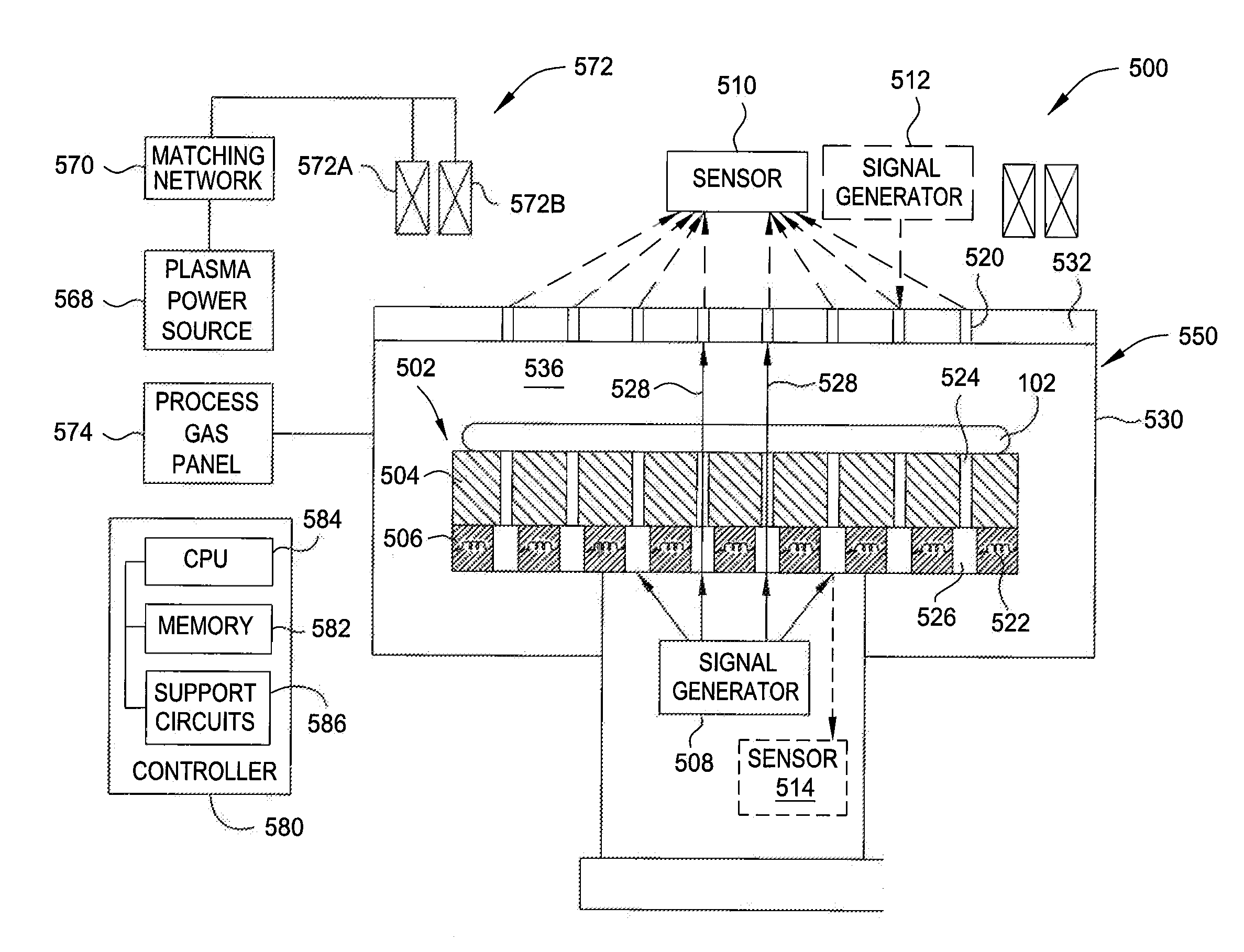
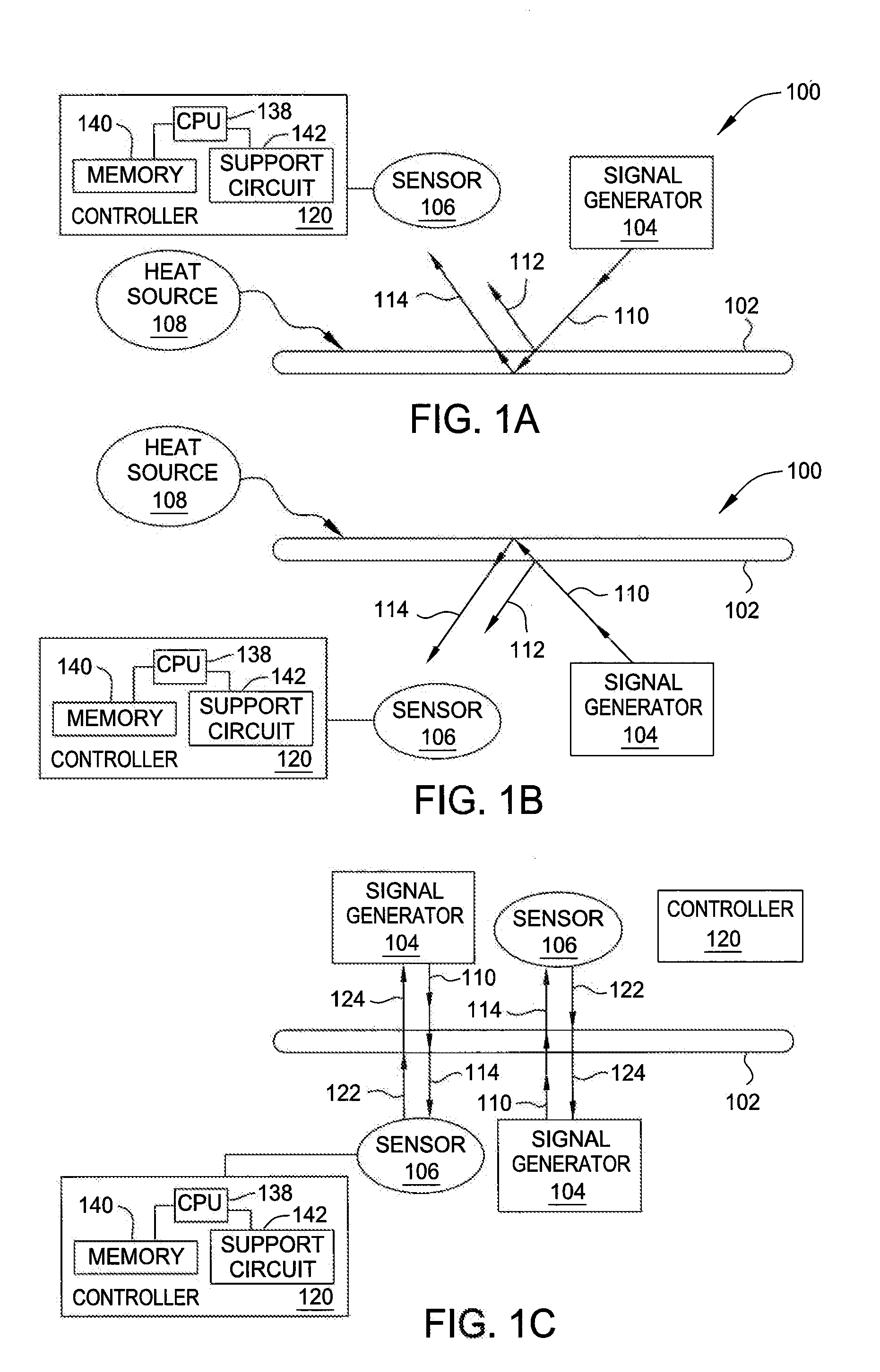
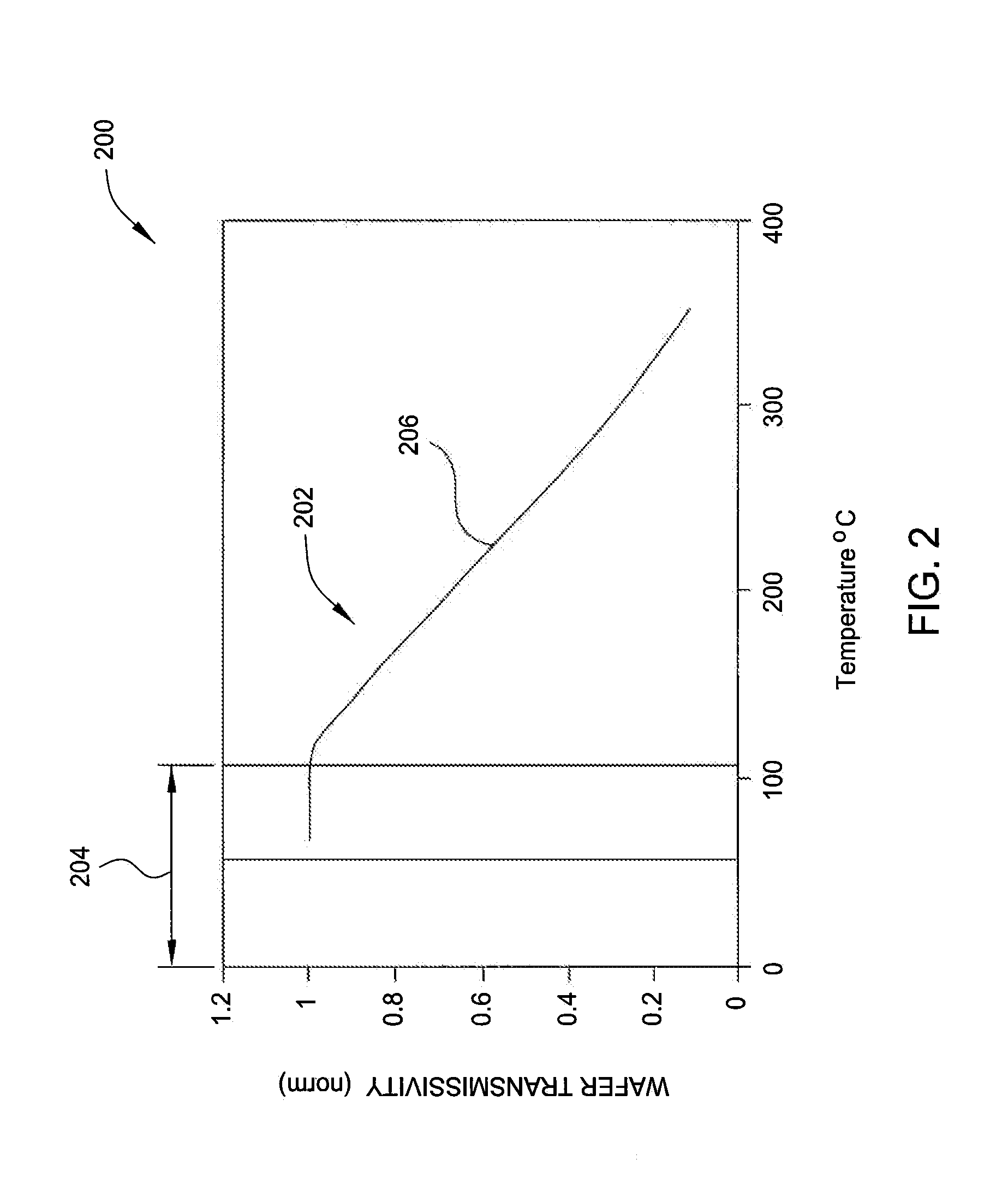
[0030]Embodiments discussed herein provide methods and apparatuses for measuring a substrate temperature during heating or cooling processes, such as may be used in etching. Other example processes may include plasma processes such as etching, deposition, annealing, plasma surface treating and ion implantation, among others. In one embodiment, the substrate temperature may be determined by monitoring the transmittance of energy through a substrate. In a further embodiment, an energy source, such as a laser emitting infrared (IR) light, may be turned on and off during a process to allow subtraction of other energy sources from the transmission measurement. Various details regarding substrate temperature measurement by infrared transmission may be found in U.S. Pat. No. 7,946,759 and in U.S. patent application Ser. No. 12 / 144,157, which are both incorporated by reference as if fully set out herein.

[0031]FIGS. 1A-1C depict a simplified schematic diagram of a processing apparatus suitab...


PUM

PropertyMeasurementUnit
wavelengthaaaaaaaaaa

Abstract

An apparatus is provided for measuring a substrate temperature during an etching process, comprising: one or more windows formed in a substrate supporting surface; a first signal generator configured to pulse a first signal; and a first sensor positioned to receive energy transmitted from the first signal generator through the one or more windows. A method is provided for measuring a substrate temperature during an etching process comprising: heating a substrate using radiant energy; pulsing a first light; determining a metric indicative of total transmittance through the substrate when the first light is pulsed on; determining a metric indicative of background transmittance through the substrate when the first light is pulsed off; and determining a process temperature.

Description

CROSS-REFERENCE TO RELATED APPLICATION / PRIORITY CLAIM[0001]This application claims the benefit of U.S. Provisional Application No. 61 / 531,327, filed on Sep. 6, 2011, which is herein incorporated by reference in its entirety.BACKGROUND OF THE INVENTION[0002]1. Field of the Invention[0003]Aspects of the present invention generally relate to a method and apparatus for measuring a semiconductor substrate temperature. Further, aspects of the present invention relate to non-contact wafer temperature measurement in an infrared heating environment. More specifically, a method and apparatus for measuring a semiconductor substrate temperature in an etch process by substrate infrared transmission.[0004]2. Description of the Related Art[0005]Ultra-large-scale integrated (ULSI) circuits may include more than one billion electronic devices (e.g., transistors) that are formed on a semiconductor substrate, such as a silicon (Si) substrate, and cooperate to perform various functions within the devic...

Claims


Application Information

Patent Timeline
Patent Type & Authority Applications(United States)
IPC IPC(8): H01L21/66H01L21/306
CPCH01L21/67248G01J5/0007H01L21/3065H01L22/00
Inventor LEE, JARED AHMADLI, JIPING
Owner APPLIED MATERIALS INC
Why Eureka
Try Eureka