Semiconductor device and method for fabricating the same

a technology of semiconductors and semiconductors, applied in the field of semiconductor devices, can solve the problems of confined application of transistors, and achieve the effect of improving performance and improving film quality

Inactive Publication Date: 2013-03-21
UNITED MICROELECTRONICS CORP
View PDF3 Cites 36 Cited by
  • Summary
  • Abstract
  • Description
  • Claims
  • Application Information

AI Technical Summary

Benefits of technology

[0006]Accordingly, the present invention is directed to a semiconductor device and a method for fabricating

Problems solved by technology

However, due to the limitations in mobility of electrons and

Method used


Image

  • Semiconductor device and method for fabricating the same
  • Semiconductor device and method for fabricating the same
  • Semiconductor device and method for fabricating the same

Examples


Embodiment Construction

[0027]Reference will now be made in detail to the present preferred embodiments of the invention, examples of which are illustrated in the accompanying drawings. Wherever possible, the same reference numbers are used in the drawings and the description to refer to the same or like parts.

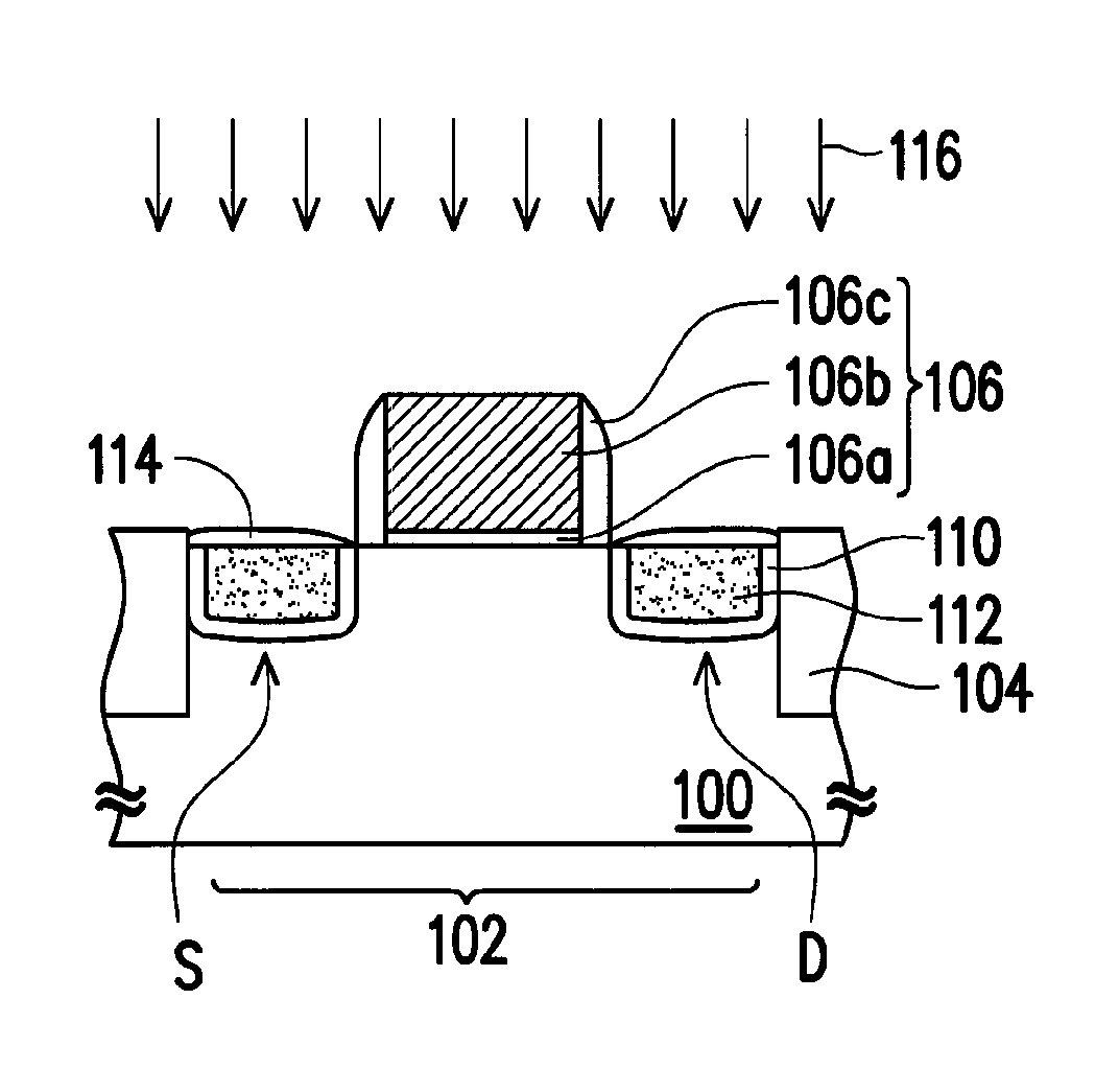
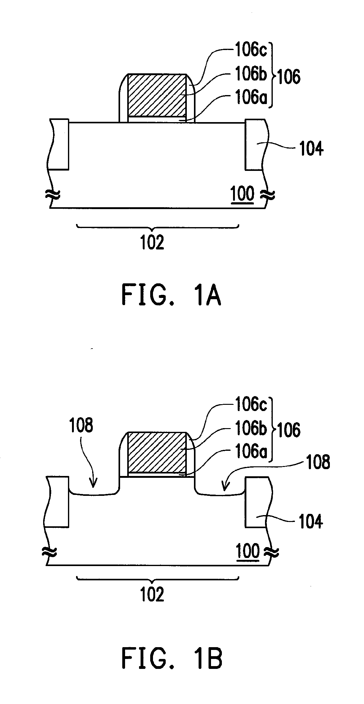
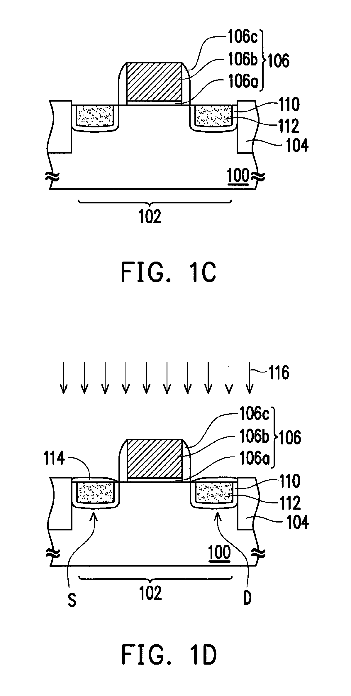
[0028]FIGS. 1A-1D depict, in a cross-sectional view, a method for fabricating a semiconductor device according to an embodiment of the present invention. Referring to FIG. 1A, a substrate 100 is provided. The substrate 100 can be a semiconductor wafer, e.g. an N- or a P-type silicon wafer. Isolation structures 104 are formed in the substrate 100, so as to define an active region 102. The isolation structures 104 are, for example, formed by shallow trench isolation (STI), and made of insulating material such as silicon oxide.

[0029]Then, a gate structure 106 is formed on the substrate 100 within the active region 102. The gate structure 106 includes a gate dielectric layer 106a, a gate 106b and a pair ...


PUM


Abstract

A semiconductor device and a method for fabricating the same are provided. The semiconductor device includes a gate structure, a source region and a drain region. The gate structure is disposed on a substrate. The source and drain regions disposed at respective sides of the gate structure include a boron-doped silicon germanium (SiGeB) layer substantially without stress relaxation. The boron-doped silicon germanium (SiGeB) layer has a germanium concentration greater than 30 at % and an in-situ doping concentration of boron ranging between 2.65×10²⁰/cm3 and 1×10²¹/cm3.

Description

BACKGROUND OF THE INVENTION[0001]1. Field of the Invention[0002]The present invention relates to a semiconductor device and a method for fabricating the same, and more particularly, to a transistor including a high Ge-content silicon germanium (SiGe) layer and a method for fabricating the same.[0003]2. Description of Related Art[0004]Metal oxide semiconductor (MOS) transistor is one of the most common elements used in many different semiconductor devices, such as memories, image sensors or displays. Along with rapid progress of semiconductor technology, dimensions of semiconductor devices are reduced and integrity thereof is promoted continuously to further advance the operating speed and performance of integrated circuits (ICs). However, due to the limitations in mobility of electrons and holes in silicon, applications of the transistor are confined.[0005]Accordingly, changing the mobility of electrons and holes by means of controlling mechanical stress in the channel is proposed t...

Claims


Application Information

Patent Timeline
IPC IPC(8): H01L29/78H01L21/336
CPCH01L29/41783H01L29/165H01L29/7848H01L29/66636
Inventor LIAO, CHIN-IHSUAN, TENG-CHUNCHIEN, CHIN-CHENG
Owner UNITED MICROELECTRONICS CORP
Why Eureka
Try Eureka