Stiction-free drying of high aspect ratio devices

Inactive Publication Date: 2013-04-04
APPLIED MATERIALS INC
View PDF11 Cites 22 Cited by
  • Summary
  • Abstract
  • Description
  • Claims
  • Application Information

AI Technical Summary

Benefits of technology

[0016]In one embodiment of the invention, the device is a NAND flash memory device which includes floating gates in a gate stack where the STI ½ pitch dimensions are 50 nm down to about 10 nm, and where the aspect ratio of the line structures in the floating gate stack ranges from about 5 up to about 20. A particularly advantageous drying liquid (drying agent) is a simple compound. We have discovered that acetone [(CH3)2CO], which is 100% water miscible and which can be recovered from the water and recycled, if desired (using distillation processes, for example) works particularly well. The drying liquid/agent is heated to or near its boiling point (56° C. for acetone at atmospheric pressure) to create a vapor which can move and flow over the surface of the devices (which are typically present on a silicon wafer substrate, for example, but may be present on other substrates as well). After a wafer surface containing the devices is DI water rinsed, the wet surface of the wafer is exposed to the acetone vapor such that acetone is condensed on the wafer surface. During application of the acetone vapor to the wafer surface, it is helpful to have the wafer surface oriented horizontally, facing the ground, with the source of the drying liquid vapor being such that the vapor rises upward to contact the wafer surface (vapor flow direction is perpendicular to the surface which is to be dried). When the tops of the features extending downward towards the ground, the benefit of gravity flow assists the condensed liquid/water solution separation from the wafer surface, as it drips off the substrate surface while fresh drying liquid vapor is condensing upon the wafer surface.

Problems solved by technology

The method relies on the use of a drying liquid which not only exhibits a low surface tension, but also exhibits a high evaporation rate.
It appears that, due to the very rapid removal of the drying liquid coa

Method used


Image

  • Stiction-free drying of high aspect ratio devices
  • Stiction-free drying of high aspect ratio devices
  • Stiction-free drying of high aspect ratio devices

Examples


Embodiment Construction

[0039]As a preface to the detailed description, it should be noted that, as used in this specification and the appended claims, the singular forms “a”, “an”, and “the” include plural referents, unless the context clearly dictates otherwise.

[0040]When the word “about” is used herein, this is intended to mean that the nominal value presented is precise within ±10%.

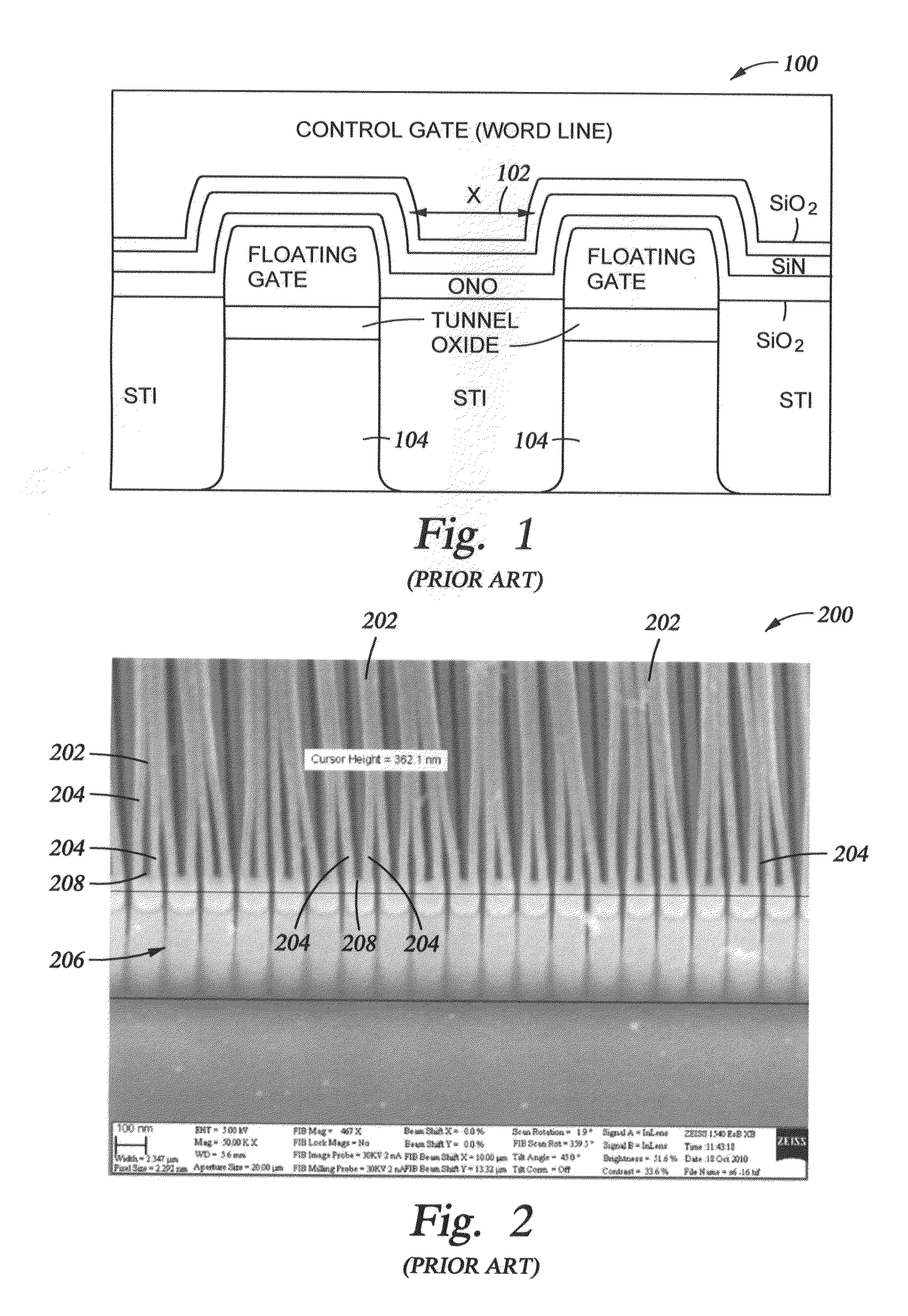
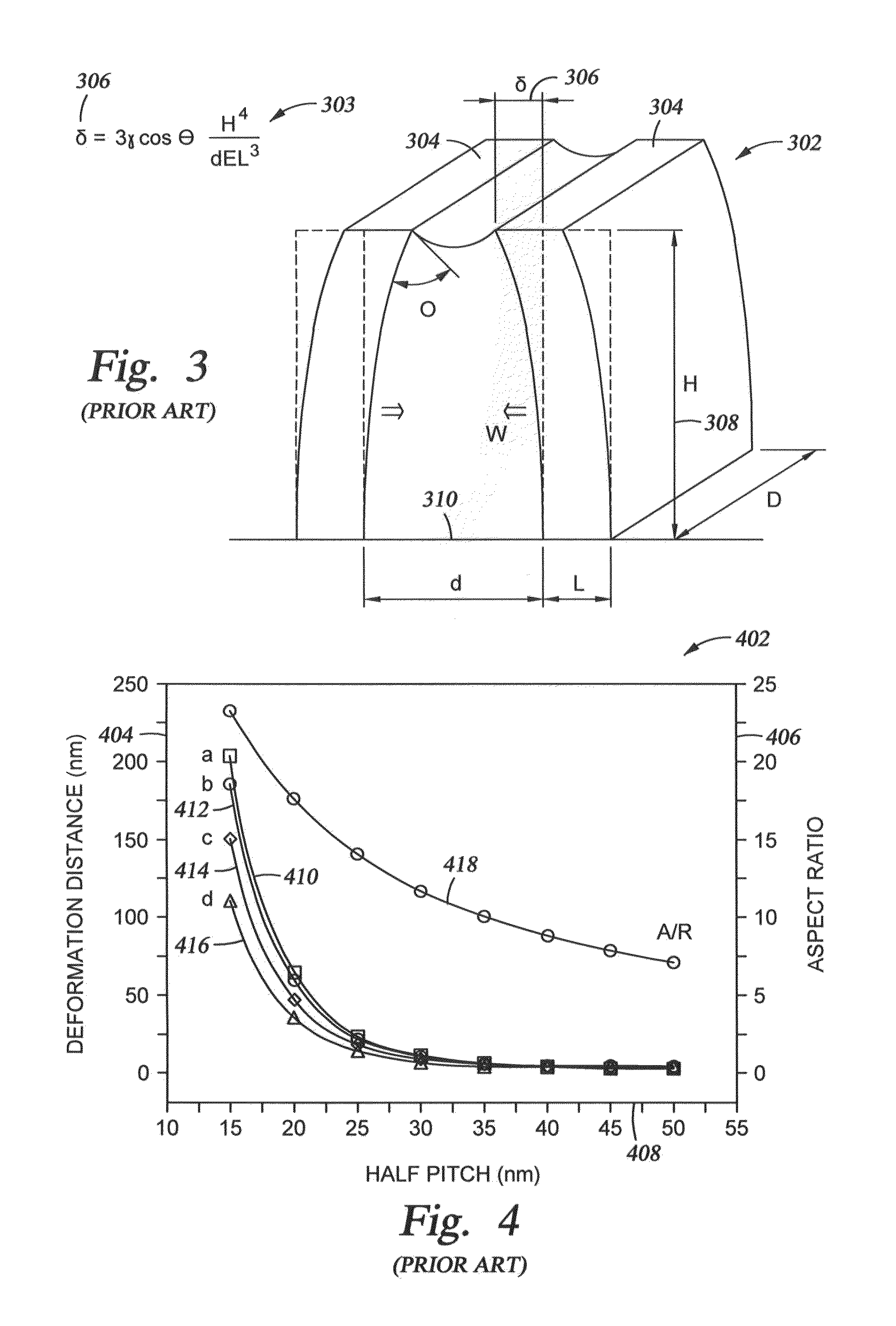
[0041]We have developed a method of removing a water-comprising rinse material from the surface of a device which includes high aspect ratio features which are separated by 50 nm or less without causing stiction between feature surfaces. The method is particularly helpful during fabrication of electronic memory storage devices, such as NAND flash memory devices, for example and not by way of limitation. The method relies on the use of a low surface tension drying liquid which also exhibits a high evaporation rate. We have discovered that by using a drying liquid having a particular surface tension combined with a particular ...


PUM


Abstract

A method of removing a water-comprising rinse/cleaning material from the surface of a device which includes high aspect ratio features (an aspect ratio of 5 or greater) where sidewalls of the feature are separated by 50 nm or less without causing stiction between the feature sidewall surfaces. The method relies on the use of a low surface tension drying liquid which also exhibits a high evaporation rate. The method also relies on a technique by which the drying liquid is applied. Increasing the evaporation rate of the drying liquid and application of the drying liquid in the form of a vapor helps to eliminate stiction.

Description

TECHNOLOGY FIELD[0001]The present application is related to a method which reduces feature sidewall collapse during wet cleaning after an etching process during semiconductor microelectronics device fabrication or during MEMS fabrication.DESCRIPTION OF THE BACKGROUND[0002]This section describes background subject matter related to the disclosed embodiments of the present invention. There is no intention, either express or implied, that the background art discussed in this section legally constitutes prior art.[0003]Feature sidewall collapse during fabrication of high aspect ratio semiconductor device structures is a particular problem when spacings between feature dimensions are below 50 nm and the feature includes sidewalls with an aspect ratio greater than about 5. This problem is frequently observed with respect to electronic memory storage devices, such as NAND flash memory devices, for example, where line structures collapse during wet cleaning and drying of the etched line str...

Claims


Application Information

Patent Timeline
IPC IPC(8): F26B3/00F26B21/14
CPCH01L29/66825H01L27/11521H01L21/02057H01L21/67034H01L21/67028H10B41/30
Inventor GOUK, ROMANVERHAVERBEKE, STEVENCHEN, HAN-WEN
Owner APPLIED MATERIALS INC
Why Eureka
Try Eureka